
Content on this page
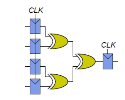
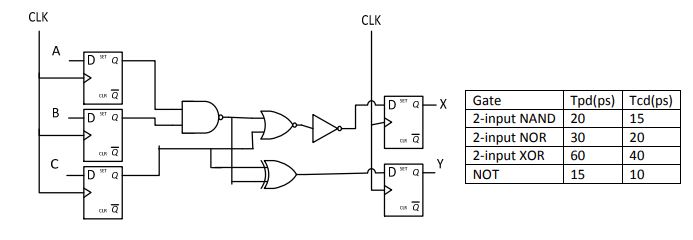
| In the following circuit Each flip flop has: Setup time of 60ps Hold time of 20ps Clock-to-Q maximum delay of 70ps Clock-to-Q minimum delay of 50ps Each XOR gate has: Propagation delay of 100ps Contamination delay of 55ps |
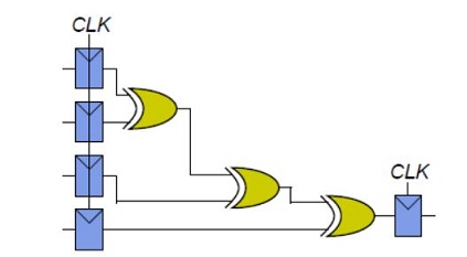 |
b. How much clock skew can the circuit tolerate before it might experience a hold time violation?
c. Redesign the circuit so that it can be operated at 3GHz frequency. How much clock skew can your circuit tolerate before it might experience a hold time violation?
Solution
a.
Longest path: Tc ≥ Tpcq + 3*Tpd + Tsetup Tc ≥ 70 + 3*100 + 60 = 430 ps Max Frequency = 1/Tc = 2.33 GHz
Shortest Path: Tccq + Tcd ≥ Thold + Tskew 50 + 55 ≥ 20 + Tskew Tskew ≤ 85 ps |
 |
Problem 2:
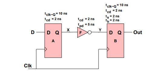
Solution
Before starting timing analysis, consider the flow of data in this circuit in response to a rising clock edge, starting at flip-flop A.1. Following the rising clock edge on Clk, a valid output appears on signal X after tClk−Q = 10 ns.
2. A valid output Y appears at the output of inverter F, tpd = 5 ns after a valid X arrives at the gate. 3. Signal Y is clocked into flip-flop B on the next rising clock edge. This signal must arrive at least ts = 2ns before the rising clock edge.
As a result, the minimum clock period, Tmin of the circuit is:
Tmin = tClk − Q(A) + tpd(F) + ts(B)
= 10ns + 5ns + 2ns = 17ns
maximum clock frequency of the circuit is 1/Tmin = 1/17ns = 58.8 MHz
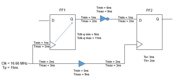
Problem 3:
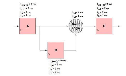
In a typical sequential circuit design there are often millions of flip-flop to flip-flop paths that need to be considered in calculating the maximum clock frequency. This frequency must be determined by locating the longest path among all the flip-flop paths in the circuit. For example, consider the circuit shown in above. there are three flip-flop to flip-flop paths (flop A to flop B, flop A to flop C, flop B to flop C),the delay along all three paths are:
- TAB = tClk−Q(A) + ts(B) = 9 ns + 2 ns = 11 ns
- TAC = tClk−Q(A) + tpd(Z) + ts(C) = 9 ns + 4 ns + 2 ns = 15 ns
- TBC = tClk−Q(B) + tpd(Z) + ts(C) = 10 ns + 4 ns + 2 ns = 16 ns
Problem 4:
• Maximum clock frequency for reliable operation.
• The amount of clock skew the circuit can tolerate if it needs to operate at 5 Ghz.
• How much clock skew the circuit can tolerate before it experiences a hold time violation?
Flip-Flop (clock-to-q) propagation delay (tpcq) = 35 ps
Flip-Flop (clock-to-q) contamination delay (tccq) = 20 ps
Flip-Flop data setup time (ts) = 30 ps
Flip-Flop data hold time (th) = 10 ps
Solution
-
a.
- Period > (FF propagation delay) + (max combination circuit delay) + (FF Setup time) + (max clock skew)
Period > 35 + (60+20) + 30 +0 ps
Period > 145 ps
F < 1/(145 ps)
F < 6.8965 GHz.
- At F= 5 GHz Period = 1/(5 Ghz) = 200 ps.
Max clock skew = Clock period – (FF propagation delay + max combination circuit delay + FF Setup time)
Max clock skew = 200 – (35 + (60+20) + 30) = 200 – 145 = 55 ps.
- For hold time violation to NOT occur.
Hold time <= (FF contamination delay) + (min combinational circuit delay) - (max clock skew)
So hold time will get violated when
Max clock skew > (FF contamination delay) + (min combinational circuit delay) – (Hold Time)
Max clock skew > 20 + (20+10) – 10
Max clock skew > 40 ps
Problem 5:
-
a. setup slack
b. hold slack
Solution
before proceeding with the solution we should know :-
setup slack = RTmin(minimum required time) - ATmax(maximum arrival time)
where; RTmin ≥ ATmax to satisfy setup time
Hold Slack = ATmin(minimum arrival time) - RTmax(maximum arrival time)
where; ATmax ≥ RTmin to satisfy hold time
a. Setup Slack
-
ATmax = 2 + 11 + 2 + 9 + 2 + 3 = 29ns
RTmin = 2+ 5 + 2 + 15(here 15ns is the time perid) = 24ns
Setup slack = ATmax - RTmin = 24 - 29 = -5ns
b. Hold Slack
-
ATmin = 1 + 9 + 1 + 6 + 1 - 2 (here Thold is considered and subtracted) = 16ns
RTmax = 3 + 9 + 3 = 15ns
Hold Slack = ATmin - RTmax = 16 - 15 = 1ns

- What is synthesis?
- Goals of synthesis
- Synthesis Flow
- Synthesis (input & output)
- HDL file gen. & lib setup
- Reading files
- Design envi. Constraints
- Compile
- Generate Reports
- Write files
- Netlist(.v or .vhd)
- Constraints
- Liberty Timing File(.lib or .db)
- Library Exchange Format(LEF)
- Technology Related files
- TLU+ File
- Milkyway Library
- Power Specification File
- Optimization Directives
- Design Exchange Formats
- Clock Tree Constraints/ Specification
- IO Information File
- import design
- sanity checks
- partitioning (flat and hierarchy)
- objectives of floorplan
- Inputs of floorplan
- Floorplan flowchart
- Floorplan Techniques
- Terminologies and definitions
- Steps in FloorPlan
- Utilization
- IO Placement
- Macro Placement
- Macro Placement Tips
- Blockages (soft,hard,partial)
- Halo/keepout margin
- Issues arises due to bad floor-plan)
- FloorPlan Qualifications
- FloorPlan Output
- levels of power distribution
- Power Management
- Powerplanning involves
- Inputs of powerplan
- Properties of ideal powerplan
- Power Information
- PowerPlan calculations
- Sub-Block configuration
- fullchip configuration
- UPF Content
- Isolation Cell
- Level Shifters
- Retention Registers
- Power Switches
- Types of Power dissipation
- IR Drop
- Electromigration
- Pre-Placement
- Pre-Placement Optimization
- Placement
- Placement Objectives
- Goals of Placement
- Inputs of Placement
- Checks Before placement
- Placement Methods(Timing & Congestion)
- Placement Steps
- Placement Optimization
- Placement Qualifications
- Placement Outputs
- Pre-CTS Optimization
- CTS
- Diff b/w HFNS & CTS
- Diff b/w Clock & normal buffer
- CTS inputs
- CTS Goals
- Clock latency
- Clock problems
- Main concerns for Clock design
- Clock Skew
- Clock Jitter
- CTS Pre requisites
- CTS Objects
- CTS Flow
- Clock Tree Reference
- Clock Tree Exceptions
- CTS Algorithm
- Analyze the Clock tree
- Post CTS Optimization
- CTS Outputs
- Importance of Routing as Technology Shrinks
- Routing Objectives
- Routing
- Routing Inputs
- Routing Goals
- Routing constraints
- Routing Flow
- Trial/Global Routing
- Track Assignment
- Detail/Nano Routing
- Grid based Routing
- Routing Preferences
- Post Routing Optimization
- Filler Cell Insertion
- Metal Fill
- Spare Cells Tie-up/ Tie-down
- Diff b/w DTA & STA
- Static Timing Analysis
- main steps in STA
- STA(input & output)
- Timing Report
- Clocked storage elements
- Delays
- Pins related to clock
- Timing Arc
- Timing Unate
- Clock definitions in STA
- Timing Paths
- Timing Path Groups
- Clock Latency
- Insertion Delay
- Clock Uncertainty
- Clock Skew
- Clock Jitter
- Glitch
- Pulse width
- Duty Cycle
- Transition/Slew
- Asynchronous Path
- Critical Path
- Shortest Path
- Clock Gating Path
- Launch path
- Arrival Path
- Required Time
- Common Path Pessimism(CPP/CRPR)
- Slack
- Setup and Hold time
- Setup & hold time violations
- Recovery Time
- Removal Time
- Recovery & Removal time violations
- Single Cycle path
- Multi Cycle Path
- Half Cycle Path
- False Path
- Clock Domain Crossing(CDC)
- Clock Domain Synchronization Scheme
- Bottleneck Analysis
- Multi-VT Cells(HVT LVT SVT)
- Time Borrowing/Stealing
- Types of STA (PBA GBA)
- Diff b/w PBA & GBA
- Block based STA & Path based STA
- Congestion Analysis
- Routing Congestion Analysis
- Placement Cong. Analysis
- Routing Congestion causes
- Congestion Fixes
- Global & local cong.
- Congestion Profiles
- Power Analysis
- Leakeage Power
- Switching Power
- Short Circuit
- Leakage/static Power
- Static power Dissipation
- Types of Static Leakage
- Static Power Reduction Techniques
- Dynamic/Switching Power
- Dynamic Power calculation depends on
- Types of Dynamic Power
- Dynamic Power Reduction Techniques
- IR Drop Analysis
- Types of IR Drop & their methodologies
- IR Drop Reasons
- IR Drop Robustness Checks
- IR Drop Impacts
- IR Drop Remedies
- Ldi/dt Effects
- Design Parasitics
- Latch-Up
- Electrostatic Discharge(ESD)
- Electromigration
- Antenna Effect
- Crosstalk
- Soft Errors
- Sef Heating
- Cells in PD
- Standard Cells
- ICG Cells
- Well Taps
- End Caps
- Filler Cells
- Decap Cells
- ESD Clamp
- Spare Cells
- Tie Cells
- Delay Cells
- Metrology Cells
- IO Pads
- Types of IO Pads
- Delay Calculation
- Delay Models
- Interconnect Delay Models
- Cell Delay Models
- Engineering Change Order
- Post Synthesis ECO
- Post Route ECO
- Post Silicon ECO
- Metal Layer ECO Example
- std cell library types
- Classification wrt density and Vth
- The Discontinuity
- Discontinuity: Classification
- DFM/DFY
- Yield Classification
- Why DFM/DFY?
- DFM/DFY Solution
- Wire Spreading
- metal Fill
- CAA
- CMP Aware-Design
- Redundant Via
- RET
- Litho Process Check(LPC)
- Layout Dependent Effects
- Resolution Enhancement Techniques
- Types of RET
- Optical Proximity Correction(OPC)
- Scattering Bars
- Multiple Patterning
- Phase-shift Masking
- Off-Axis Illumination
- Corners
- Need for corner analysis
- PVT Variations
- Corner Analysis
- PVT/RC Corners
- Temperature Inversion
- Cross Corner Analysis
- Modes of Analysis
- MC/MM Analysis
- OCV
- Derating
- OCV Timing Checks
- OCV Enhancements
- AOCV
- SSTA
- CRPR/CPPR
