Short Channel Effect in MOSFET

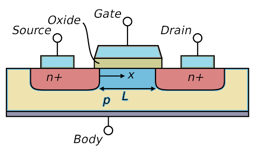
MOSFET = Metal oxide semiconductor field effect transistor
  • It has 2 regions at each edge of MOSFET called source and Drain.
  • A terminal called Gate exist in between the source and drain.
  • pn Junction is formed between source/drain and substrate n/p type materials.

What is Short Channel ?

  • Short channel is the depletion channel length between the source and drain,
  • therefore, a MOSFET device is considered to be short when channel length is the same order of magnitude as the depletion-layer widths (XdD, XdS) of the source and drain junction.
  • As the channel length L is reduced. then it is so called short-channel length arise.
  • However.. it has pros and cons

PROS and CONS (short channel effect)

    pros :

    It leads MOSFET has a good processing speed, requires low operating potential and increases transistor density on the chip.

    cons :

    It faces som serious issues like Drain induced barrier lowering and punchthrough(DIBL), Surface Scattring, Velocity saturation, impact ionization, hot electron effect.

Drain Induced Barrier Lowering(DIBL)

  • The source and drain depletion regions can intrude into the channel even without bias, as these junctions are brought closer together in short channel devices.
  • This effect is called charge sharing since the source and drain in effect take part of the channel charge, which would otherwise be controlled by the gate.
  • As the drain depletion region continues to increase with the bias, it actually interact with the source junction and hence lowers the potential barrier.
    When the source junction barrier is reduced, electrons are easily injected into the channel and the gat voltage has no longer any control over the drain current.

Surface Scattering

  • When th carriers travel along the channel they are attracted to the surface by the elctric field creatd by the gate voltage.
  • As a result, they keep crashing and bouncing against the surface, during their travel, following a zig-zagging path.
  • This effectively reduces the surface mobility of the carriers. In comparison with their bul mobility. the change in carrier mobility impacts the current- voltage relationship of the transistor.
  • As the electron travels through the channel. It is attracted to the silicon to silicon dioxide interface and bounce against it. this effect reduces its mobility.

Velocity Saturation

  • The performance of short channel devices is also affcted by the velocity saturation, which reduces the transconductance in saturation mode.
  • At low ey, the value of drift velocity VDE is varies linearity with the elctric field intensity.
  • This is because the value of ey increases will cause the drift velocity tends to increase more slowly, and approaches a saturation value.
  • The drain current is limited by velocity saturation instead of pitch off. this occurs i short cannel devices when the dimnsions are scaled without lowering the bias voltags.

Impact Ionization

  • When an electron collides with an atom of the silicon lattice structure, the energy passed to the atom upon collision can knock out an electron out of the valence band to the conduction band, creating an electron-hole pair.
  • The hole is attracted to the bulk while the generated electron moves on to the drain.
  • An undesirable short channel effect, especially in NMOS. Occurs due to the high velocity of electrons.
  • In the prresense of high longitudical fields, it can generate electron-hole(e-h) pairs by impact ionization that is by impacting on silicon atoms and ionizing them.

Hot Electrons/Carrier Injection

  • Hot electron effect is the transport of the energetic electrons over (or tunneling through) the barrier into the oxide.
  • Such the electrons become trapped in the oxide layer, where they change the threshold voltage and V-I characteristics of the device.
  • This give rise to oxide charging that can accumulate with time and degrade the device performance by increasing VT and affect adversely the gate's control on the drain current.

This can be reduced by a few ways as below

  • using high intensity light during masking
  • by optical proximity correction
  • Thinning gate oxide and using shallow source or drain junctions.
  • By making a novel self-aligned double-gate MOSFETs.
  • What is synthesis?
  • Goals of synthesis
  • Synthesis Flow
  • Synthesis (input & output)
  • HDL file gen. & lib setup
  • Reading files
  • Design envi. Constraints
  • Compile
  • Generate Reports
  • Write files
Go To page
  • Netlist(.v or .vhd)
  • Constraints
  • Liberty Timing File(.lib or .db)
  • Library Exchange Format(LEF)
  • Technology Related files
  • TLU+ File
  • Milkyway Library
  • Power Specification File
  • Optimization Directives
  • Design Exchange Formats
  • Clock Tree Constraints/ Specification
  • IO Information File
Go To page
  • import design
  • sanity checks
  • partitioning (flat and hierarchy)
  • objectives of floorplan
  • Inputs of floorplan
  • Floorplan flowchart
  • Floorplan Techniques
  • Terminologies and definitions
  • Steps in FloorPlan
  • Utilization
  • IO Placement
  • Macro Placement
  • Macro Placement Tips
  • Blockages (soft,hard,partial)
  • Halo/keepout margin
  • Issues arises due to bad floor-plan)
  • FloorPlan Qualifications
  • FloorPlan Output
Go To page
  • levels of power distribution
  • Power Management
  • Powerplanning involves
  • Inputs of powerplan
  • Properties of ideal powerplan
  • Power Information
  • PowerPlan calculations
  • Sub-Block configuration
  • fullchip configuration
  • UPF Content
  • Isolation Cell
  • Level Shifters
  • Retention Registers
  • Power Switches
  • Types of Power dissipation
  • IR Drop
  • Electromigration
Go To page
  • Pre-Placement
  • Pre-Placement Optimization
  • Placement
  • Placement Objectives
  • Goals of Placement
  • Inputs of Placement
  • Checks Before placement
  • Placement Methods(Timing & Congestion)
  • Placement Steps
  • Placement Optimization
  • Placement Qualifications
  • Placement Outputs
Go To page
  • Pre-CTS Optimization
  • CTS
  • Diff b/w HFNS & CTS
  • Diff b/w Clock & normal buffer
  • CTS inputs
  • CTS Goals
  • Clock latency
  • Clock problems
  • Main concerns for Clock design
  • Clock Skew
  • Clock Jitter
  • CTS Pre requisites
  • CTS Objects
  • CTS Flow
  • Clock Tree Reference
  • Clock Tree Exceptions
  • CTS Algorithm
  • Analyze the Clock tree
  • Post CTS Optimization
  • CTS Outputs
Go To page
  • Importance of Routing as Technology Shrinks
  • Routing Objectives
  • Routing
  • Routing Inputs
  • Routing Goals
  • Routing constraints
  • Routing Flow
  • Trial/Global Routing
  • Track Assignment
  • Detail/Nano Routing
  • Grid based Routing
  • Routing Preferences
  • Post Routing Optimization
  • Filler Cell Insertion
  • Metal Fill
  • Spare Cells Tie-up/ Tie-down
Go To page
  • Diff b/w DTA & STA
  • Static Timing Analysis
  • main steps in STA
  • STA(input & output)
  • Timing Report
  • Clocked storage elements
  • Delays
  • Pins related to clock
  • Timing Arc
  • Timing Unate
  • Clock definitions in STA
  • Timing Paths
  • Timing Path Groups
  • Clock Latency
  • Insertion Delay
  • Clock Uncertainty
  • Clock Skew
  • Clock Jitter
  • Glitch
  • Pulse width
  • Duty Cycle
  • Transition/Slew
  • Asynchronous Path
  • Critical Path
  • Shortest Path
  • Clock Gating Path
  • Launch path
  • Arrival Path
  • Required Time
  • Common Path Pessimism(CPP/CRPR)
  • Slack
  • Setup and Hold time
  • Setup & hold time violations
  • Recovery Time
  • Removal Time
  • Recovery & Removal time violations
  • Single Cycle path
  • Multi Cycle Path
  • Half Cycle Path
  • False Path
  • Clock Domain Crossing(CDC)
  • Clock Domain Synchronization Scheme
  • Bottleneck Analysis
  • Multi-VT Cells(HVT LVT SVT)
  • Time Borrowing/Stealing
  • Types of STA (PBA GBA)
  • Diff b/w PBA & GBA
  • Block based STA & Path based STA
Go To page

  • Congestion Analysis
  • Routing Congestion Analysis
  • Placement Cong. Analysis
  • Routing Congestion causes
  • Congestion Fixes
  • Global & local cong.
  • Congestion Profiles
Go To page
  • Power Analysis
  • Leakeage Power
  • Switching Power
  • Short Circuit
  • Leakage/static Power
  • Static power Dissipation
  • Types of Static Leakage
  • Static Power Reduction Techniques
  • Dynamic/Switching Power
  • Dynamic Power calculation depends on
  • Types of Dynamic Power
  • Dynamic Power Reduction Techniques
Go To page
  • IR Drop Analysis
  • Types of IR Drop & their methodologies
  • IR Drop Reasons
  • IR Drop Robustness Checks
  • IR Drop Impacts
  • IR Drop Remedies
  • Ldi/dt Effects
Go To page

  • Design Parasitics
  • Latch-Up
  • Electrostatic Discharge(ESD)
  • Electromigration
  • Antenna Effect
  • Crosstalk
  • Soft Errors
  • Sef Heating
Go To page
  • Cells in PD
  • Standard Cells
  • ICG Cells
  • Well Taps
  • End Caps
  • Filler Cells
  • Decap Cells
  • ESD Clamp
  • Spare Cells
  • Tie Cells
  • Delay Cells
  • Metrology Cells
Go To page
  • IO Pads
  • Types of IO Pads
Go To page
  • Delay Calculation
  • Delay Models
  • Interconnect Delay Models
  • Cell Delay Models
Go To page
  • Engineering Change Order
  • Post Synthesis ECO
  • Post Route ECO
  • Post Silicon ECO
  • Metal Layer ECO Example
Go To page
  • std cell library types
  • Classification wrt density and Vth
Go To page

  • The Discontinuity
  • Discontinuity: Classification
  • DFM/DFY
  • Yield Classification
  • Why DFM/DFY?
  • DFM/DFY Solution
  • Wire Spreading
  • metal Fill
  • CAA
  • CMP Aware-Design
  • Redundant Via
  • RET
  • Litho Process Check(LPC)
  • Layout Dependent Effects
  • Resolution Enhancement Techniques
  • Types of RET
  • Optical Proximity Correction(OPC)
  • Scattering Bars
  • Multiple Patterning
  • Phase-shift Masking
  • Off-Axis Illumination
Go To page
  • Corners
  • Need for corner analysis
  • PVT Variations
  • Corner Analysis
  • PVT/RC Corners
  • Temperature Inversion
  • Cross Corner Analysis
  • Modes of Analysis
  • MC/MM Analysis
  • OCV
  • Derating
  • OCV Timing Checks
  • OCV Enhancements
  • AOCV
  • SSTA
  • CRPR/CPPR
Go To page
Copyright © 2021