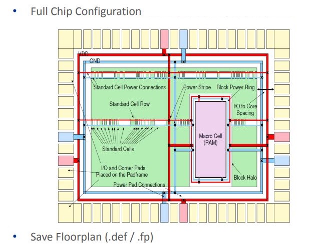
To connect Power to the Chip by considering issues like EM and IR Drop
Power Routing also called Pre-Routing
Pre-Routing includes creating Power Ring, Stripes/Mesh/Grid, and Standard Cell Power Rails
Power Planning also includes Power Via insertion
IO Rings are established through IO Cell abutment and through IO Filler Cells
Power Trunks are constructed between Core Power Ring and Power Pads
Technical information required for Power Planning:
Total Dynamic Power info. will get from Compiler
Technology File will provide Current Density (JMAX)
LEF will prove the Metal Layer width
Technology Library will provide Core Voltage
Levels of Power Distribution
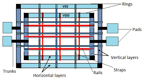
Rings
VDD and VSS Rings are formed around the Core and Macro
Stripes
Carries VDD and VSS around the chip
Carries VDD and VSS from Rings across the chip
Power Stripes are created in the Core Area to tap power from Core Rings to the core area
Rails (Special Route)
Connect VDD and VSS to the standard cell
Standard Cell Rails are created to tap power from Power Stripes to Std. Cell Power/Ground Pins
Power Vias
Insert all Power Vias between Ring & Grid, Grid & Rail and Vertical Grid & Horizontal Grid
Trunks
Connects Ring to Power Pad
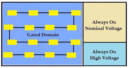
Core Power Management
VDD and VSS power rings are formed around the core and macro. In addition to this straps and trunks are
created for macros as per the power requirement. Std cell rails are created to tap power from power straps to
std cell power/ground pins. I/O Power Management
Power rings are formed for I/O cells and trunks are constructed between core power ring and power pads.
Power Planning Involves
calculating number of power pins required
Number of Rings, Stripes
width of ring and stripes
IR Drop
Inputs of Power plan
Netlist & SDC
.lib , .lef & tech file
Tlu+ file
UPF
Ideal Power distribution network has the following properties
maintain a stable voltage with little noise
Avoid wear out from EM and self heating
Consume little chip area and wiring
Easy to layout
Power Information
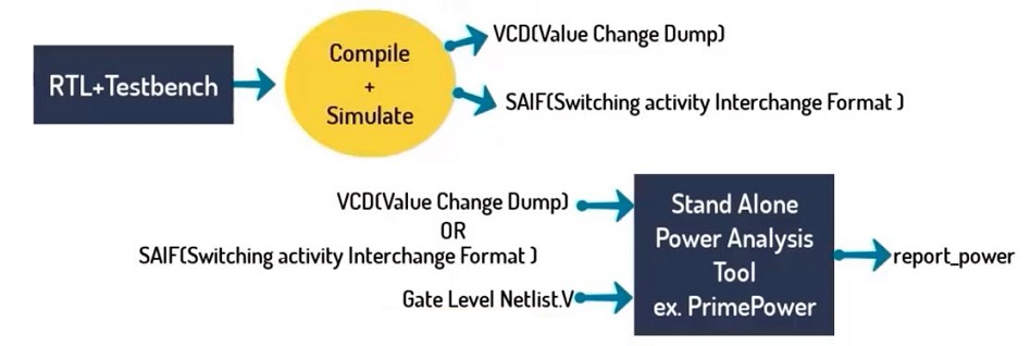
The power information can obtain from the front end design.
the synthesis tool reports static power information
dynamic power can be calculated using value change dump (VCD) or switching activity interchange format (SAIF) file in conjunction with RTL description and test bench.
Exhaustive test coverage is required for efficient calculation of peak power. this methodology is depicted in figure as shown below.
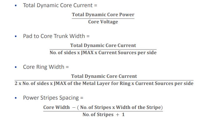
PowerPlan : Calculations
UPF Contents
Power intent specifies
Power Distribution Architecture:
Power domains – Group of elements which share a common set of power supply requirements
Supply rails – Power distribution (ports, nets, sets & switches)
Shutdown control
Power Strategy
Power state tables – Legal combination of states of each power domain
Operating voltages
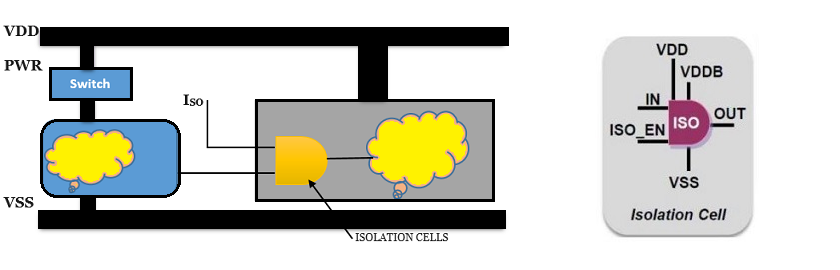
Usage of Special cells
Isolation cells
Level shifters
Power switches
Retention registers
Isolation cells
Powered off domains do not drive their outputs anymore and these outputs become floating nodes. This
could be a problem when other active domains gets these floating nodes as input. It could result in crowbar
current which affects the proper functioning of the powered up domain.
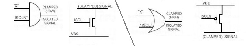
Isolation cells (also called “clamps”) keep the turned off sub-block outputs at a predefined value. This is how
the shut-down sub-block does not corrupt other active sub-block functionality.
Isolation cells are powered by a constant supply and drive 0, 1 or latch the old value of the turned off
domain.
Isolation cells pass logic values during the normal mode of operation, but clamp it to some specified value
when a control signal is asserted.
Isolation cell clamps the output of powered down block to a specified value (‘0’, ‘1’, last)
Gate type clamp cells (AND, OR)
Transistor type clamp (pull-up, pull-down)
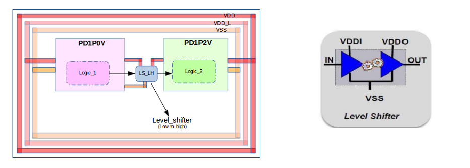
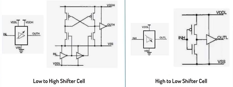
Level Shifters
Level shifters have the minimal functionality of a buffer.
Necessary as most low-power designs have multi-voltage domains and/or employ dynamic voltage scaling.
A level shifter swings a logic value in one voltage domain to the same logic value in another voltage domain.
An ‘Up’ level shifter swings a logic value from a lower voltage domain to the same logic value in a higher voltage domain.
A ‘Down’ level shifter swings a logic value from a higher voltage domain to the same logic value in a lower voltage domain.
Internal circuit of level shifter.
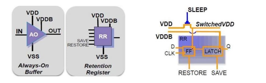
Retention Registers
In order to reduce power consumption, memories are shut down where their power domain is switched off or when they are not in use. Registers are corrupted when power is switched off. Corruption is typically represented as ‘X’ (unknown).
Some memories need to retain their values for fast wake-up. For these memories, only the memory array stays powered on during the shut-down while the peripheral interfaces are powered off.
Retention registers keep their previous active value after being shut down.
Retention registers save state information before a power domain is switched off and restore it when the power is turned back on.
Retention registers comprise of two circuits.
Standard register logic, supplied by primary power VDD
Shadow latch retention circuitry, with alternate supply VDDB
SAVE – transfers FF content into shadow latch during shutdown
RESTORE – transfers state from shadow latch to FF when powered back on
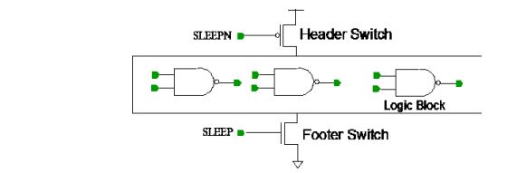
Power Switches
Power switches are required to Gate the power supply of gated domain when not required. power switches are MT-CMOS (Multi Threshold) cells, which will have very high threshold
voltage when device is OFF & very low threshold voltage when deviceis ON.
power switches are inserted in power mesh & supply to all gated domain cells will be through power switches. hence a single/few switches are not enough. A strong network of power switchs connected
in daisy chain fashion will be inserted in the design.
There are 2 types of power switches
header and
footer
Header
The header switch is implemented by PMOS transistors to control Vdd supply.
PMOS transistor is less leaky than NMOS transistor of a same size. Header switches turn off VDD and keep VSS on. As the result, it allows a simple design of a pull-down transistor to isolate power-off cells and clamp output signals
The disadvantage of the header switch is that PMOS has lower drive current than NMOS of a same size, though difference is reduced by strained silicon technology. As a result, a header switch implementation usually consumes more area than a
footer switch implementation.
Footer
The footer switch is implemented by NMOS transistor to control VSS supply.
The advantage of footer switch is the high drive and hence smaller area.
However, NMOS is leakier than PMOS and a Designs become more sensitive to ground noise
Frequently Used Power Reduction Techniques
Power Gating:
In a processor chip, certain areas of the chip will be idle and will be activated only for certain operations. But these areas are still provided with power for biasing.
The power gating limits this unnecessary power being wasted by shuting down power for that area and resuming whenever needed.
It is used for reducing LEAKAGE POWER or power consumption by switching off power supply to the non operational power domain of the chip during certain mode of operation.
Header & footer switches, isolation cells, state retention flip flops are used for implementing power gating.
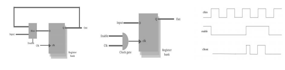
Clock Gating:
Clock gating limits the clock from being given to every register or flops in the processor. It disables the clock of an unused device. In clock gating the gated areas will still be provided with bias power.
It is used for reducing DYNAMIC POWER by controlling switching activities on the clock path.
Generally gate or latch or flip flop based block gating cells are used for implementing clock gating.
50% of dynamic power is due to clock buffer. Since clock has highest toggle rate and often have higher drive strength to minimize clock delay. And the flops receive clocks dissipates some dynamic power even if input and output remains the same. Also clock buffer tree consumes power. One of the techniques to lower the dynamic power is clock gating.
In load enabled flops, the output of the flops switches only when the enable is on. But clock switches continuously, increasing the dynamic power consumption.
By converting load enable circuits to clock gating circuit dynamic power can be reduced. Normal clock gating circuit consists of an AND gate in the clock path with one input as enable. But when enable becomes one in between positive level of the clock a glitch is obtained.
To remove the glitches due to AND gate, integrated clock gate is used. It has a negative triggered latch and an AND gate.
Clock gating makes design more complex. Timing and CG timing closure becomes complex. Clock gating adds
more gates to the design. Hence min bit width (minimum register bit width to be clock gated) should be wisely
chosen, because the overall dynamic power consumption may increase.
Voltage and Frequency Scaling:
It changes the voltage and clock frequency to match the performance requirements for a given operation so as to minimize leakage.
Different blocks are operated at variable supply voltages. The block voltage is dynamically adjusted based on performance requirements.
Frequency of the block is dynamically adjusted. Works alongside with voltage scaling. Substrate Biasing:
It changes the threshold voltage to reduce leakage current at the expense of slower switching times.
Multiple Threshold Voltages:
Uses different Vt in the circuit to reduce leakage but still satisfy timing constraints.
Multiple Supply Voltages:
Using Multi VDD reduces power consumption by powering down the not used voltage domain. Different
blocks are operated at different supply voltages. Signals that cross voltage domain boundaries have to be level
shifted.
Memory Partitioning:
The memory is split into several partitions. Not used ones can be powered down.
Types of Power Dissipation:
The power dissipation is classified in two categories:
Static power dissipation
Dynamic power dissipation
Static Power Dissipation:
In this class, power will be dissipated irrespective of frequency and switching of the system. It is continuous and
has become more dominant at lower node technologies. The structure and size of the device results in various
leakage currents.
Few reasons for static power dissipation are:
Sub-threshold current
Gate oxide leakage
Diode reverse bias current
Gate induced leakage
Its hard to find the accurate amount of leakage currents but it mainly depends on supply voltage (VDD),
threshold voltage (Vth), transistor size (W/L) and the doping concentration.
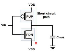
Dynamic Power Dissipation:
There are two reasons of dynamic power dissipation; Switching of the device and short circuit path from supply
(VDD) to ground (VSS). This occurs during operation of the device. Signals change their logic state charging and
discharging of output mode capacitor.
Short-circuit Power Dissipation:
Because of slower input transition, there will be certain duration of time “t”, for which both the devices (PMOS
and NMOS) are turned ON. Now, there is a short circuit path from VDD to VSS. This short circuit power is given
by:
Pshort-circuit = Vdd. Isc. t
where, Vdd – Supply voltage, Isc – Short-circuit current and t – Short-circuit time.
Short-circuit power is directly proportional to rise time and fall time.
Switching Power Dissipation:
Energy is drawn from the power supply to charge up the output mode capacitance. Charging up of the output
cap causes transition from 0V to VDD. So, the power dissipated during charging and discharging of total load
[output capacitance + net capacitance + input capacitance of driven cell(s)] is called Switching power
dissipation. The switching power is given by:
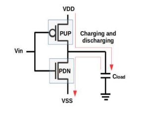
Pswitch = α·VDD2 · Cload·f
where, α – Switching activity factor, f – Operating frequency,
VDD – Supply voltage & Cload – Load capacitance.
Fundamental sources of power supply noise are IR Drop & Ldi/dt noise.
IR Drop
the power supply in the chip is distributed uniformly through metal layers across the design and these metal layers have their finite amount of resistance.
when we applied the volatge the current starts flowing through these metal layers and some voltage is dropped due to that resistance of a metal wire and current.
this drop is called IR Drop. Because of IR drop, delay will increase and it violates the timing and this will increase noise and performance will be degraded.
There are 2 types of IR Drop.
Static IR Drop: This drop is independent of cell switching and this is calculated with the help of metal own resistance.
Dynamic IR Drop: This drop is calculated with the help of the switching of cells. when a cell is switching at the active edge of the clock the cell requires large current or voltage
to turn on but due to voltage drop suffficient amount of voltage is not reached to thr particular cell and cell may be goes into metastable state and effect the timing and performance.
Methods to improve static IR Drop
We can go for higher layers if available.
Increase the width of the straps.
Increase the number of wires.
Check if any via is missing then add more via.
Methods to improve Dynamic IR Drop
Use De-Cap Cells.
Increase the number of straps.
Tools Used for IR Drop Analysis
Redhawk from Apache
Volatage storm from cadence
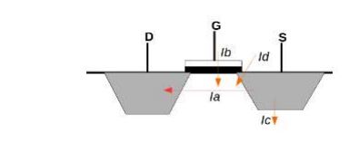
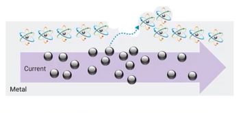
Electromigration
When a high density of current is flowing through metal layers, the atoms (electron) in the metal layers are displaced from their origional position causing open and shorts in the metal layers.
Heating also accelerates EM because higher temperature cause a high number of metal ions to diffuse
In higher technology nodes we saw the EM on power and clock metal layers but now in lower nodes the signal metal layers are also needed to be analyzes due to an increased amount of current density.
clock nets are more prone to EM because they have high switching activity because of this only we are avoiding to use high drive strength clock buffers to build the clock tree.