Design Rule Check (DRC) is the process of checking physical layout data against fabrication-specific rules specified by the foundry to ensure successful fabrication.
Process specific design rules must be followed when drawing layouts to avoid any manufacturing defects during the fabrication of an IC.
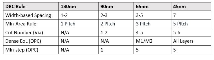
Process design rules are the minimum allowable drawing dimensions which affects the X and Y dimensions of layout and not the depth/vertical dimensions.
As Technology Shrinks
Number of Design Rules are increasing
Complexity of Routing Rules is increasing
Increasing the number of objects involved
More Design Rules depending on Width, Halo, Parallel Length
Violating a design rule might result in a non-functional circuit or low Yield.
Design Rule examples
Maximum Rules: Manufacturing of large continuous regions can lead to stress cracks. So ‘wide metal’ must be ‘slotted’ (holes)
Angles: Usually only multiples of 45 degree are allowed
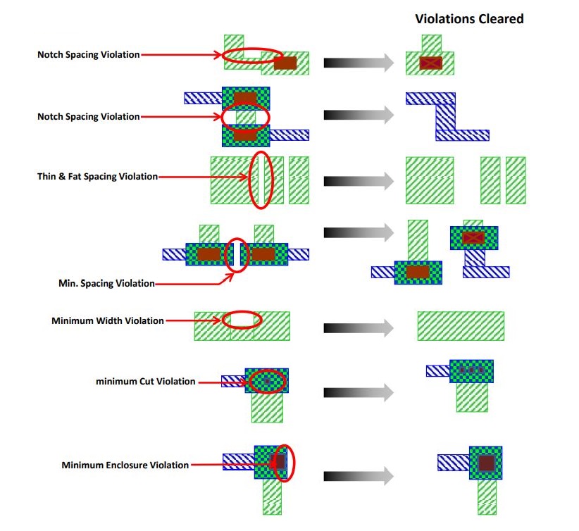
Grid: All corner points must lie on a minimal grid, otherwise an “off griderror” is produced
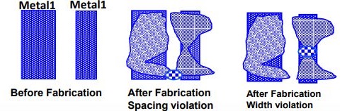
Minimum Spacing: The minimum spacing between objects on a single layer
Minimum Width: The min width rule specifies the minimum width of individual shapes on a single layer
Minimum Enclosure/ Overlap: Implies that the second layer is fully enclosed by the first one
Notch: The rule specifies the minimum spacing rule for objects on the same net, including defining the minimum notch on a single-layer, merged object
Minimum Cut: the minimum number of cuts a via must have when it is on a wide wire
DRC have 2 categories – Base Layer DRC's and Metal DRC's
Base Layer DRC's:
Base layer means all layers upto contact/metal 1. In Base layer, DRC flow rules will be checked:
Base DRC's are spacing rules for geometries inside transistor (Well spacing, Poly spacing, Poly width)
Tap cell requirement
Well continuity (after routing fill empty space using spare cells)
Fixes:
Make sure design is placed legally
No cell overlaps & no gaps
Most of the times, base DRC’s will be clean if we ensure above two conditions.
Metal DRC's:
Metal DRC means from contact to all the routing layers. Basic metal DRC's are:
Width (min & max)
Spacing (min)
Via enclosure (size of min cut, min via to via spacing in multi cut Vias)
Layout Versus Schematic (LVS)
DRC only verifies that the given layout satisfies the design rules provided by the fabrication unit. It does not
ensure the functionality of layout. Because of this, idea of LVS is originated.
LVS Flow
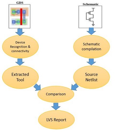
Layout Versus Schematic (LVS) verifies the connectivity of a Verilog Netlist and Layout Netlist (Extracted Netlist from GDS)
Tool extracts circuit devices and interconnects from the layout and saved as Layout Netlist (SPICE format)
As LVS performs comparison between 2 Netlist, it does not compare the functionalities of both the Netlist.
Input Requirements
LVS Rule deck
Verilog Netlist
Physical layout database (GDS)
Spice Netlist (Extracted by the tool from GDS)
LVS rule deck is a set of code written in Standard Verification Rule Format (SVRF) or TCL Verification Format
(TVF). It guides the tool to extract the devices and the connectivity of IC’s. It contains the layer definition to
identify the layers used in layout file and to match it with the locaƟon of layer in GDS. It also contains device
structure definitions.
LVS checks examples
Short Net Error, Open Net Error, Extract errors, Compare errors
Steps of LVS
Extraction: The tool takes GDSII file containing all the layers and uses polygon based approach to
determine the components like transistors, diodes, capacitors and resistors and also connectivity information
between devices presented in the layout by their layers of construction. All the device layers, terminals of the
devices, size of devices, nets, vias and the locations of pins are defined and given an unique identification.
Reduction: All the defined information is extracted in the form of netlist.
Comparison: The extracted layout netlist is then compared to the netlist of the same stage using the LVS
rule deck. In this stage the number of instances, nets and ports are compared. All the mismatches such as
shorts and opens, pin mismatch etc.. are reported. The tools also checks topology and size mismatch.
LVS Checks
No of devices in schematic and its layout
Type of devices in schematic and its layout
No of nets in schematic and its layout
Errors occur
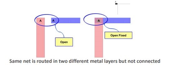
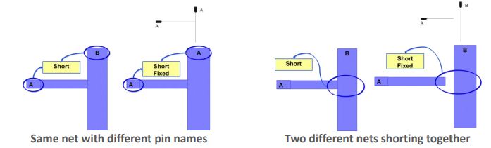
Shorts: Shorts are formed, if two or more wires which should not be connected together are connected.
Opens: Opens are formed, if the wires or components which should be connected together are left floating or partially connected.
Component mismatch: Component mismatch can happen, if components of different types are used (e.g, LVT cells instead of HVT cells).
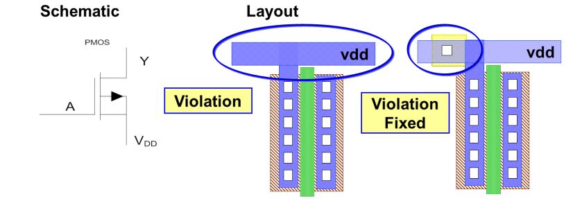
Missing components: Component missing can happen, if an expected component is left out from the layout.
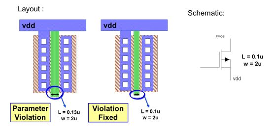
Parameter mismatch: All components has it’s own properties, LVS tool is configured to compare these properties with some tolerance. If this tolerance is not met, then it will give parameter mismatch.
LVS checks examples : Short Net Error, Open Net Error, Extract errors, Compare errors
Open Net Error
Short Net Error
Extract Errors
Parameter Mismatch
Device parameters on schematic and layout are compared
Example: Let us consider a transistor here, LVS checks are necessary parameters like width, length, multiplication factor etc.
Compare Errors
Malformed Devices
Pin Errors
Device Mismatch
Net Mismatch
Electrical Rule Check (ERC)
Electrical Rule Check (ERC) is used to analyze or confirm the electrical connectivity of an IC design
ERC checks are run to identify the following errors in layout
To locate devices connected directly between Power and Ground
To locate floating Devices, Substrates and Wells
To locate devices which are shorted
To locate devices with missing connections
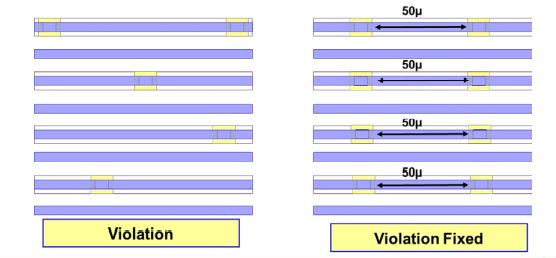
Well Tap connection error: The Well Taps should bias the Wells as specified in the schematics
Well Tap Density Error: If there is no enough Taps for a given area then this error is flagged
Taps need to be placed regularly which biases the Well to prevent Latch-up
e.g., In typical 90nm process the Well Tap Density Rule require Well-taps to be placed every 50 microns
Tools: Mentor Graphics Calibre, Synopsys Hercules, Cadence Assura, Magma Quartz
Lithography Process Checking (LPC)
The scaling of advanced process node design rules has progressed faster than the reduction in lithographic exposure wavelength available for high-volume wafer fabrication.
As a result, two key characteristics have evolved:
The mask data differs (rather drastically) from the tapeout physical database. The mask data adjustments have evolved throughout process node generations.
Initially, a set of optical proximity corrections (OPC) were applied, mostly to improve the exposure fidelity of the corners of drawn shapes.
In subsequent process nodes, a set of sub-resolution assist features (SRAFs) were added to the mask data, separate from the drawn layout,
to provide constructive and destructive interference illumination intensity when exposing the photoresist-coated wafer. Presently, an extremely complex set of algorithms,
known as source-mask optimization (SMO), are applied to derive both the mask data and the (non-uniform) exposing illumination pattern.
Layout design rules became much more complex. The layout data are now subject to an increasing set of design rules that arise from lithographic exposure resolution requirements
or fabrication uniformity constraints:
Forbidden pitches
Additional dummy shapes required adjacent to active circuits to improve local exposure uniformity (e.g., unconnected active and gate fill shapes data)
Limited ranges for allowed dimensions of devices, contacts, vias, and wires for both improved exposure and etch uniformity (either a narrow range of continuous dimensions or, more commonly, a set of allowed discrete values)
Increasingly, the layout data for devices and local metals resembles an optical grating, with restrictions on segments in the non-preferred direction.
These two factors introduce a non-trivial risk that a tapeout layout database may be DRC clean yet present difficulties during mask data preparation to find a suitable SMO solution. For advanced process nodes, the foundries have introduced a new physical verification methodology flow requirement to perform LPC.
The foundry and EDA vendor collaborate closely to define a set of high-risk layout topologies to use with the LPC tool pattern matching features. In addition, the foundry may provide SMO-like algorithms to the EDA vendor to embed into the LPC software to further reduce the risk of an incomplete solution during subsequent mask data preparation. This combination of pattern (“rule”) checking and algorithm (“model”) analysis is computationally expensive. Further, LPC is really applicable just prior to tapeout. The assumption is that the design rules will indeed be sufficient, and the LPC flow will not uncover any SMO-related errors on the tapeout database. As a result, it would be unnecessary (and expensive) to exercise LPC on each successive version release of physical data during the design phase of the SoC schedule. Further, the set of LPC patterns and SMO models from the foundry evolves as the new process node matures; it is necessary to exercise LPC on the latest foundry PDK runset during the SoC schedule tapeout phase.
Because the demand for LPC software licenses is sporadic and the (full chip) computational resources are substantial, EDA vendors commonly provide LPC physical verification as a separate services business rather than lease on-premises software licenses. Thus, the EDA vendor chosen for stand-alone LPC verification could be separate from the provider of DRC, LVS, and ERC tools. The selection would likely be based on contracted services cost, availability of computational resources (that align with the SoC tapeout schedule), and verification turnaround time.
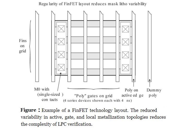
With the increasingly restrictive design rules for new process nodes, the SMO data preparation risk is likely to be adequately addressed by the rule-based, pattern-matching method, obviating the need for the model-based analysis. The layout regularity associated with FinFET fins, device gates, solution during subsequent mask data preparation. This combination of pattern (“rule”) checking and algorithm (“model”) analysis is computationally expensive. Further, LPC is really applicable just prior to tapeout. The assumption is that the design rules will indeed be sufficient, and the LPC flow will not uncover any SMO-related errors on the tapeout database. As a result, it would be unnecessary (and expensive) to exercise LPC on each successive version release of physical data during the design phase of the SoC schedule. Further, the set of LPC patterns and SMO models from the foundry evolves as the new process node matures; it is necessary to exercise LPC on the latest foundry PDK runset during the SoC schedule tapeout phase.
Because the demand for LPC software licenses is sporadic and the (full chip) computational resources are substantial, EDA vendors commonly provide LPC physical verification as a separate services business rather than lease on-premises software licenses. Thus, the EDA vendor chosen for stand-alone LPC verification could be separate from the provider of DRC, LVS, and ERC tools. The selection would likely be based on contracted services cost, availability of computational resources (that align with the SoC tapeout schedule), and verification turnaround time.
With the increasingly restrictive design rules for new process nodes, the SMO data preparation risk is likely to be adequately addressed by the rule-based, pattern-matching method, obviating the need for the model-based analysis. The layout regularity associated with FinFET fins, device gates, and wiring track multipatterning color pre-assignment reduces the custom layout variability, as depicted in Figure
LPC flow execution as a tapeout prerequisite may be achievable solely by applying pattern-matching features, using (existing) DRC software licenses.
DRC Waivers
A fabrication process evolves over time. Preproduction design rules from the PDK v0.x release versions are used by “early adopters” of the technology (e.g., IP developers, leading-edge customers) who want to have designs ready for volume ramp when the PDK v1.0 release is available. During this evolution, the fab is working on establishing a process window that results in suitable wafer-level yield across the manufacturing variations in deposition, lithography, and etch steps. Design rule updates in PDK v0.x releases may result.
After the PDK v1.0 release, the process continues to evolve as the foundry engineers pursue continuous process improvement (CPI) efforts to maximize yield and reduce costs. Again, design rule changes may be present in PDK releases v1.1, v2.0, and so on. As a result, designs verified to an earlier PDK release may have DRC violations when integrated into a subsequent SoC tapeout. An SoC project manager and foundry product engineering team need to review whether a DRC waiver will be applied. Such a waiver represents an assessment by the foundry that the wafer yield will not be adversely impacted. For the SoC design team, the waiver request would be made only if the resource required to address the DRC error (and recharacterize the design) would have an impact on the tapeout schedule. The SoC project manager may commit to removing the waiver request in a subsequent tapeout if the prototype tapeout is allowed to proceed on its current schedule.
There are two project methodology aspects to addressing potential DRC waivers:
Early identification prior to tapeout—To avoid schedule delays at tapeout while the foundry reviews a DRC waiver request, the project schedule should include full-chip DRC flow evaluation during preliminary physical integration steps. Some project managers include a mock physical tapeout milestone. Although this activity is resource intensive, the early identification of potential DRC waiver requests is critical to minimizing tapeout review delays at the foundry.
During the SoC design phase, if a new PDK release is provided by the foundry, existing IP is re-validated. Any new DRC violations need to be reviewed to assess whether a layout update (and re-characterization) or a DRC waiver request should be pursued. This resource and schedule impact assessment is complicated by the use of design IP from external suppliers; their resource availability to update and rerelease a new IP version may or may not coincide with the SoC tapeout schedule. (This dependency on external vendor IP rerelease is especially problematic if new IP silicon testsite characterization is warranted.)
Project database management of DRC waivers—The SoC project database maintains information about the PDK version used for verification of all library IP. In addition, the database includes all existing waivers that have been granted by the foundry. When the SoC design data and physical verification flow results are being compiled for tapeout submission, DRC errors need to be cross-referenced to the waivers in the project database and included in the supplementary tapeout materials. The prototype fabrication TAT from tapeout submission is used to establish project schedule dates for silicon bring-up tasks and resources. Any additional delays due to unsuccessful review of the tapeout materials at the foundry have a direct impact on that schedule. Appropriate project management of (requested and granted) waivers is critical.