Physical Design Q&A

Q431. Explain the concept of a lockup latch?

The latch lockup is the concept in STA where a higher clock skew is present. The lockup latch is just like a transparent latch, which is placed at that point, where clock skew is maximum. To reduce the clock skew and follow the hold time constraints, the lockup latch is used, during design for testability. The Figure shows the concept of lockup latch.
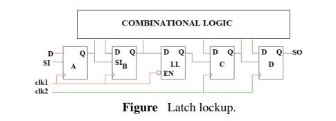

The clock skew occurs mostly in the systems where multiple clocks are used. The clock skew can occur during shift and capture time. The clock skew can be minimized during a shift by grouping all the flip-flops which are run by the same clock. To remove clock skew completely, the lockup latch should be inserted where the domains cross. This will solve the problem of clock skew during shift.

In scan-chain, the lockup latch will act as an end-point. The scan chain can be reordered, by grouping the cells from starting to lockup latch as one domain, and from lockup, latch to the last cell as a second domain. That way makes the clock grouping preserved.

The timing path will be divided as:
    Domain 1: Launch flip-flop to lockup latch
    Domain 2: Lockup latch to capture flip-flop
The lockup latch can be placed in between cells automatically or by using a scan chain order file.
There may be multiple clock paths between clock domains that are available during capture. The clock skew during capture can be reduced by a pulse one clock per pattern.

Q432. If the clock skew is large, can you use buffers to avoid hold time constraints violation?

It is discouraged practice to use the buffers when clock skew is large. As the number of buffers will be increased, which will automatically degrade the performance of the circuit as area and power factor will also be enhanced. It will increase the chances of on-chip variation (OCV). The optimized solution for handling large clock skew and hold time constraints is the insertion of a lockup latch.

Q433. What are the advantages of a lockup latch?

  1. It is power and area efficient.
  2. The device can handle more OCV (on-chip variation) easily.
  3. This is the robust method to deal with hold time constraints during scan shift mode.
  4. It prevents data corruption i.e. data overridden which occurs due to clock skew.

Q434. Is there any difference between the lockup latch and lockup register?

As the lockup latch occupies approximately half of the area than the lockup register, so lockup latch is having an optimized solution in terms of power and area as compared to the lockup register. During negative lockup latch, there is no need to worry about timing constraints at functional frequency. But this is not for the lockup register. So, the lockup latch is more prevalent than lockup register, during the design process and timing analysis.

Q435. What do you understand by the term ‘clock latency’?

When there is a difference between the arrival of the clock from source to pin. It is further divided into source latency and network latency. Network latency measures how fast the network is running and source latency specifies the propagation delay from the source of the clock to clock port.

Q.436. Is the term clock skew and global skew the same?

No, the clock skew and global skew both are different in terms of connections. The global skew is related to skew in between two mutually exclusive flipflops, i.e. which are not related by fan-in or fan-out. The skew between two independent flip-flops is known as global skew, whereas the skew in between two dependent flip-flops are known as clock skew.

Q.437. Can you fix the timing path? If yes, then give at least three ways to fix the timing path?

Yes, timing paths can be fixed. It can be done by any of the following ways:
  1. Logic optimization
  2. Use of macros
  3. Placement of logic/capture/launch flip-flop
  4. Pipeline can be enhanced
  5. Replicate drivers and split number of receiving gates
  6. Divide large serial operation into multiple smaller length parallel operations.
  7. Switch to the cells having low threshold voltage, high gate leakage, and fast speed.
  8. Use one hot encoding register, that will increase the speed of operation.
  9. Use power trade-off techniques.
  10. Physical design techniques to reduce capacitance and speed up the wire delays.

Q.438. What is a false path in static timing analysis?

The false path refers to a path that is not required to be optimized during timing analysis. It means it is not necessary to complete the capture and launch a task in the same clock cycle. It is known as a false path. It is not optimized by the timing optimization tool.

Q.439. What is one hot encoding method?

In the one-hot encoding technique, the number of flip-flops is increased and combinational logic is minimized. It is a state assignment method in a finite state machine. It assigns one flip-flop to each state of FSM. The number of interconnections between logic gates is reduced, which further reduces the propagation delay and speed up the finite state machine.

Q.440. . What is the concept of a multicycle path?

Usually, the data setup and hold operation are done during a single clock pulse. But there are some cases where launch and capture can take more than one clock cycle i.e. combinational delay between launch and capture edge is more than one cycle. This is known as a multicycle and timing path through this combinational logic is known as the multicycle path. Although the data is captured during the same clock cycle, in the case of the multicycle path, the capture edge of flip-flop becomes active after a specific number of cycles. Similarly, the designer will take care of the fact that data will be launched not after every single clock cycle. In such cases, the timing tool will be provided by exception or overridden flag so that it can postpone the launch and capture check after one clock cycle.

  • What is synthesis?
  • Goals of synthesis
  • Synthesis Flow
  • Synthesis (input & output)
  • HDL file gen. & lib setup
  • Reading files
  • Design envi. Constraints
  • Compile
  • Generate Reports
  • Write files
Go To page
  • Netlist(.v or .vhd)
  • Constraints
  • Liberty Timing File(.lib or .db)
  • Library Exchange Format(LEF)
  • Technology Related files
  • TLU+ File
  • Milkyway Library
  • Power Specification File
  • Optimization Directives
  • Design Exchange Formats
  • Clock Tree Constraints/ Specification
  • IO Information File
Go To page
  • import design
  • sanity checks
  • partitioning (flat and hierarchy)
  • objectives of floorplan
  • Inputs of floorplan
  • Floorplan flowchart
  • Floorplan Techniques
  • Terminologies and definitions
  • Steps in FloorPlan
  • Utilization
  • IO Placement
  • Macro Placement
  • Macro Placement Tips
  • Blockages (soft,hard,partial)
  • Halo/keepout margin
  • Issues arises due to bad floor-plan)
  • FloorPlan Qualifications
  • FloorPlan Output
Go To page
  • levels of power distribution
  • Power Management
  • Powerplanning involves
  • Inputs of powerplan
  • Properties of ideal powerplan
  • Power Information
  • PowerPlan calculations
  • Sub-Block configuration
  • fullchip configuration
  • UPF Content
  • Isolation Cell
  • Level Shifters
  • Retention Registers
  • Power Switches
  • Types of Power dissipation
  • IR Drop
  • Electromigration
Go To page
  • Pre-Placement
  • Pre-Placement Optimization
  • Placement
  • Placement Objectives
  • Goals of Placement
  • Inputs of Placement
  • Checks Before placement
  • Placement Methods(Timing & Congestion)
  • Placement Steps
  • Placement Optimization
  • Placement Qualifications
  • Placement Outputs
Go To page
  • Pre-CTS Optimization
  • CTS
  • Diff b/w HFNS & CTS
  • Diff b/w Clock & normal buffer
  • CTS inputs
  • CTS Goals
  • Clock latency
  • Clock problems
  • Main concerns for Clock design
  • Clock Skew
  • Clock Jitter
  • CTS Pre requisites
  • CTS Objects
  • CTS Flow
  • Clock Tree Reference
  • Clock Tree Exceptions
  • CTS Algorithm
  • Analyze the Clock tree
  • Post CTS Optimization
  • CTS Outputs
Go To page
  • Importance of Routing as Technology Shrinks
  • Routing Objectives
  • Routing
  • Routing Inputs
  • Routing Goals
  • Routing constraints
  • Routing Flow
  • Trial/Global Routing
  • Track Assignment
  • Detail/Nano Routing
  • Grid based Routing
  • Routing Preferences
  • Post Routing Optimization
  • Filler Cell Insertion
  • Metal Fill
  • Spare Cells Tie-up/ Tie-down
Go To page
  • Diff b/w DTA & STA
  • Static Timing Analysis
  • main steps in STA
  • STA(input & output)
  • Timing Report
  • Clocked storage elements
  • Delays
  • Pins related to clock
  • Timing Arc
  • Timing Unate
  • Clock definitions in STA
  • Timing Paths
  • Timing Path Groups
  • Clock Latency
  • Insertion Delay
  • Clock Uncertainty
  • Clock Skew
  • Clock Jitter
  • Glitch
  • Pulse width
  • Duty Cycle
  • Transition/Slew
  • Asynchronous Path
  • Critical Path
  • Shortest Path
  • Clock Gating Path
  • Launch path
  • Arrival Path
  • Required Time
  • Common Path Pessimism(CPP/CRPR)
  • Slack
  • Setup and Hold time
  • Setup & hold time violations
  • Recovery Time
  • Removal Time
  • Recovery & Removal time violations
  • Single Cycle path
  • Multi Cycle Path
  • Half Cycle Path
  • False Path
  • Clock Domain Crossing(CDC)
  • Clock Domain Synchronization Scheme
  • Bottleneck Analysis
  • Multi-VT Cells(HVT LVT SVT)
  • Time Borrowing/Stealing
  • Types of STA (PBA GBA)
  • Diff b/w PBA & GBA
  • Block based STA & Path based STA
Go To page

  • Congestion Analysis
  • Routing Congestion Analysis
  • Placement Cong. Analysis
  • Routing Congestion causes
  • Congestion Fixes
  • Global & local cong.
  • Congestion Profiles
Go To page
  • Power Analysis
  • Leakeage Power
  • Switching Power
  • Short Circuit
  • Leakage/static Power
  • Static power Dissipation
  • Types of Static Leakage
  • Static Power Reduction Techniques
  • Dynamic/Switching Power
  • Dynamic Power calculation depends on
  • Types of Dynamic Power
  • Dynamic Power Reduction Techniques
Go To page
  • IR Drop Analysis
  • Types of IR Drop & their methodologies
  • IR Drop Reasons
  • IR Drop Robustness Checks
  • IR Drop Impacts
  • IR Drop Remedies
  • Ldi/dt Effects
Go To page

  • Design Parasitics
  • Latch-Up
  • Electrostatic Discharge(ESD)
  • Electromigration
  • Antenna Effect
  • Crosstalk
  • Soft Errors
  • Sef Heating
Go To page
  • Cells in PD
  • Standard Cells
  • ICG Cells
  • Well Taps
  • End Caps
  • Filler Cells
  • Decap Cells
  • ESD Clamp
  • Spare Cells
  • Tie Cells
  • Delay Cells
  • Metrology Cells
Go To page
  • IO Pads
  • Types of IO Pads
Go To page
  • Delay Calculation
  • Delay Models
  • Interconnect Delay Models
  • Cell Delay Models
Go To page
  • Engineering Change Order
  • Post Synthesis ECO
  • Post Route ECO
  • Post Silicon ECO
  • Metal Layer ECO Example
Go To page
  • std cell library types
  • Classification wrt density and Vth
Go To page

  • The Discontinuity
  • Discontinuity: Classification
  • DFM/DFY
  • Yield Classification
  • Why DFM/DFY?
  • DFM/DFY Solution
  • Wire Spreading
  • metal Fill
  • CAA
  • CMP Aware-Design
  • Redundant Via
  • RET
  • Litho Process Check(LPC)
  • Layout Dependent Effects
  • Resolution Enhancement Techniques
  • Types of RET
  • Optical Proximity Correction(OPC)
  • Scattering Bars
  • Multiple Patterning
  • Phase-shift Masking
  • Off-Axis Illumination
Go To page
  • Corners
  • Need for corner analysis
  • PVT Variations
  • Corner Analysis
  • PVT/RC Corners
  • Temperature Inversion
  • Cross Corner Analysis
  • Modes of Analysis
  • MC/MM Analysis
  • OCV
  • Derating
  • OCV Timing Checks
  • OCV Enhancements
  • AOCV
  • SSTA
  • CRPR/CPPR
Go To page
Copyright © 2021