Q31. Why we are not checking the hold before CTS?
Before CTS, clock is ideal that means exact skew is not there. All the clocks reaching the flops at the same time. So, we don’t have skew and transition numbers of the clock path, but this information is sufficient to perform setup analysis since setup violations depends on the data path delay. Clock is propagated only after CTS (actual clock tree is built, clock buffers are added & clock tree hierarchy, clock skew, insertion delay comes into picture) and that's why hold violations are fixed only after CTS.
Q32. Can both Setup and Hold violations occur in same start and end points?
Yes, if they have different combo paths.
Q33. What is the derate value that can be used?
- For setup check derate data path by 8% to 15%, no derate in the clock path.
- For hold check derate clock path by 8% to 15%, no derate in the data path.
Q34. What are the corners you check for timing sign-off? Is there any changes in the derate value for each corner?
- Corners: Worst, Best, Typical.
- Same derating value for best and worst. For typical it can be less.
Q35. Where do you get the WLM's? Do you create WLM's? How do you specify?
- Wire Load Models (WLM) are available from the library vendors.
- We dont create WLM.
- WLMs can be specified depending on the area.
Q36.Where do you get the derating value? What are the factors that decide the derating factor?
- Based on the guidelines and suggestions from the library vendor and previous design experience derating value is decided.
- PVT variation is the factor that decides the derating factor.
Q37. Setup Fixes during placement and Setup and hold fixes during CTS?
SETUP FIXES
During Placement Stage:
- Timing path groups: We can use this option to resolve Setup timing during placement stage. Groups a set of paths or endpoints for cost function calculations. The delay cost function is the sum of all groups (weight * violation), where violation is the amount for which setup was violated for all paths within the group. If there is no violation within a group, its cost is zero. Groups enable you to specify a set of paths to optimize even though there might be larger violations in another group. When endpoints are specified, all paths leading to those endpoints are grouped.
ICC Syntax:
group_path [-weight weight_value] [-critical_range range_value] -name group_name [-from
from_list] [-through through_list] [-to to_list]
Eg: group_path -name "group1" -weight 2.0 -to {CLK1A CLK1B}
- Create Bounds: We can constrain the placement of relative placement cells by defining move bounds
with fixed coordinates. Both soft bounds and hard bounds are supported for relative placement cells, and both
rectangular bounds and rectilinear bounds are supported. To constrain relative placement by using move
bounds, use the create_bounds command.
ICC Command:
create_bounds -coordinate {100 100 200 200} "U1 U2 U3 U4" -name bound1
- If the design is having timing violation, we can rerun place_opt with the -timing and -effort high options.
ICC Command: place_opt -mtiing-driven -effort high
Timing driven placement tries to place cells along timing critical paths close together to reduce net RCs and meet setup timing.
- Change the Floorplan (macros placement, macros spacing and pin orientation) to meet the better timing.
During CTS Stage
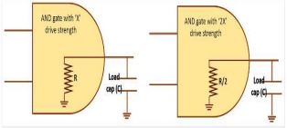
- Increase the drive strength of data-path logic gates: A cell with better drive strength can charge the load
capacitance quickly, resulting in lesser propagation delay. Also, the output transition should improve resulting in
better delay of proceeding stages. A better drive-strength gate will have a lesser resistance, effectively lowering
the RC time constant; hence, providing less delay. This is illustrated in figure below. If an AND gate of drive
strength 'X' has a pull down resistance equivalent to 'R', the one with drive strength '2X' will have R/2
resistance. Thus, a bigger AND gate with better drive strength will have less delay.

- Use data-path cells with lower threshold voltages: HVT Swap. Means change HVT cells into SVT/RVT or
into LVT. Low Vt decreases the transition time and so propagation delay decreases. So, replace HVT with RVT or
LVT will speed up the timing.
- Buffer insertion – If net length is long, then we insert Buffer to boast. It decreases the transition time,
which decreases the wire delay. If the amount of wire delay decreases due to decreasing of transition time >
cell delay of buffer, then overall delay decreases.
- Reduce the amount of buffering in the path: It will reduce the cell delay but increase the wire delay. So,
if we can reduce more cell delay in comparison to wire delay, the effective stage delay increases.
- Route the net using Higher metal layers
- Replace buffers with 2 inverters: Adding inverter decreases the transition time 2 times then the existing
buffer gate. Due to that, the RC delay of the wire decreases. Cell delay of 1 buffer gate = cell delay of 2 inverter
gate.
- Play with clock skew: Positive skew helps improve the setup slack. So, to fix setup violation, we may
either choose to increase the clock latency of capturing flip-flop, or decrease the clock latency of launching flipflop. However, in doing so, we need to be careful regarding setup and hold slack of other timing paths that are
being formed from/to these flip-flops. This is called Useful Skew. So, basically, Useful skew is nothing but adding
delay intentionally in the clock path in order to meet the better timing.
Ways to fix Hold Violation
Hold violation is just opposite of setup violation. Hold violation happens when data is too fast compared to the clock speed. For fixing the hold violation, delay should be increased in the data path.
- Increase the drive strength of data-path logic gates
- Use data-path cells with higher threshold voltages
- Buffer insertion/removal
- Route the net using Higher metal layers
- Increase the clk->q delay of launching flip-flop
Q38. Why don’t you derate the clock path by -10% for worst corner analysis?
We can do. But it may not be accurate as the data path derate.
Q39. What are the importance and need of an MMMC file in VLSI physical design?
- Multi-Mode Multi corner (MMMC) file during the physical design gives the analysis of the design over varied modes & corners.
- VLSI design can be modeled in either functional or test mode etc., with each mode at varied process corners.
- We need to ensure that the design is stable across all corners, to be specific in Tech terms PVT Corners (Process, Voltage & Temperature).
- During the process flow of physical design, (prescribed Tool-Cadence, synopsys etc.) MMMC file takes all relevant details for obtaining the desired design.
Q40. What are Timing DRV/'s, explain the Causes and its fixes?
Timing Drvs :
- Max Tran
- Max Cap
- Max Fanout
Causes:
- HVT cells give slower transition: The HVT cells have larger threshold voltages compared to LVTs and
RVTs. Hence, they take more time to turn ON resulting in larger transition time.
- Weak Driver: The driver won’t be able to drive the load resulting in bad transition of the driven cell.
Thus the delay increases.
- Load is more: The driving cell cannot drive load more that what it is characterized for. This is set in .lib
using max cap value. If the load that a cell sees increases beyond its maximum capacitance value, then it causes
bad transition and hence increases delay.
- Net length is large: Larger the net length, larger the resistance, worser the transition. Thus results in
trans violation. The RC Value of a long net will increase the load seen by a cell causing max cap violations as
well.
- Fanout is too large: If the fanout number increases beyond the limit of what the driver cell in
characterized for, it causes max fanout violations. The increased load results in max cap violation which
indirectly causes max tran violation as well.
Fixes:
Max Tran:
- Replace HVT cells with LVT cells.
- Up size the driver.
- Reduce the net length by adding buffers. Longer the nets, larger the resistance. Puting a buffer at the middle of a long net splits the resistance into half.
- Reduce the load by reducing fanout and downsizing the driven cell.
Max Cap:
- Up size the driver.
- Split long nets by buffering.
- Reduce the load by reducing the fanout (by load spliting) or by downsizing the driven cell.
Max Fanout:
- Reduce the fanout by load spliting by buffering or cloning.


