Article by Ankit Mahajan

Pessimism and Optimism in Timing Analysis


"Too much optimism or too much pessimism can negatively impact one's progress. There should always be a balance."


The above line holds equally true even in the world of VLSI industry.😂 A little pessimism is not dangerous but is helpful in meeting the timing of a design. The closest example I can come up with to explain this scenario is that If someone is able to succeed when the circumstances are slightly against him, he will definitely perform well when the circumstances are in favor. A slightly pessimistic constraints are provided to the tool so that we don't get to see any surprises in silicon. But remember that anything in excess is bad. Any extra pessimism in the timing analysis increases the effort of tool to fix the critical timing paths and can negatively impact the other parameters like power and area. On the other hand, optimism in timing analysis might result in the silicon failure. It is therefore necessary to remove extra pessimism and optimism from timing analysis.

Need of adding pessimism:

Simple explanation is that perfection can't be achieved in the practical scenario.😎 Same cells present at the different parts of the chip can have different delay values under the same operating condition. The fabrication process is not an ideal process and due to non ideal nature, the same cell at different parts of the chip will have a variation in its structure which results in the different delay numbers. Other than fabrication process, other reason for adding pessimism in the design is due to the difference in the temperature at different parts of chip due to formation of hotspots. To take this into account beforehand in EDA tools itself, OCV is considered and derates are applied to the design.

How pessimism is added to the design?

Timing engineers add pessimism to the design with the help of derates. Derates are applied on the launch clock path and capture clock path. Derate value is decided based on the guidelines and suggestions of the library vendor according to the previous fabrication experience and PVT conditions. With the refinement of the fabrication process, the value of derates becomes less pessimistic.

Setup analysis (Late analysis):

Consider a Register to Register timing path as shown in the figure below. Let's say all the cells shown below have a delay of 1ns. Now, to model On-chip variation, 10% of derate is applied. Due to the derate application the best delay value of the cell is 0.9ns and worst delay value is 1.1ns. Let's consider Tclk as 3.5ns and Tsetup = 0.6ns

To make condition more pessimistic for setup analysis, launch path is delayed (worst delay value) and the capture path is advanced (best delay value).
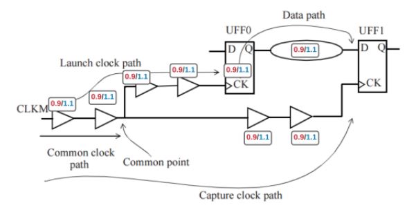

Worst scenario for setup analysis:

Launch path delay: 1.1 + 1.1 + 1.1 + 1.1 + 1.1 + 1.1 = 6.6ns
Capture path delay: 0.9 + 0.9 + 0.9 + 0.9 + 3.5 - 0.6 = 6.5ns
Setup slack = 6.5-6.6 = -0.1ns (Setup Violation)

But if you notice the two common buffers present in the clock path have different delay values in launch clock path (1.1) and capture clock path (0.9). How can a same cell have two different delay values at the same time. Taking two delay values for the same cell adds extra pessimism to the design which needs to be adjusted. The adjusted value is called as CPPR value.
CPPR = (1.1+1.1) - (0.9+0.9) = 0.4ns

Setup analysis with CPPR adjustment:

Consider one value for the common cells in the common path, say, 1.1ns. The revised equations would be
Launch path delay: 1.1 + 1.1 + 1.1 + 1.1 + 1.1 + 1.1 = 6.6ns
Capture path delay: 1.1 + 1.1 + 0.9 + 0.9 + 3.5 - 0.6 = 6.9ns
Slack = +0.3 (MET)

The setup slack in without CPPR adjustment was -0.1ns but after doing the CPPR adjustment the setup slack value is +0.4ns. There was an extra undue pessimism added in the first case which was removed in the second case. As you can see that the slack value is -ve in the first case with extra pessimism and is +ve when the extra pessimism is removed. If the extra pessimism would not have adjusted, the path would have violated and the tool would have needed more time to fix this path, unnecessarily.
  • What is synthesis?
  • Goals of synthesis
  • Synthesis Flow
  • Synthesis (input & output)
  • HDL file gen. & lib setup
  • Reading files
  • Design envi. Constraints
  • Compile
  • Generate Reports
  • Write files
Go To page
  • Netlist(.v or .vhd)
  • Constraints
  • Liberty Timing File(.lib or .db)
  • Library Exchange Format(LEF)
  • Technology Related files
  • TLU+ File
  • Milkyway Library
  • Power Specification File
  • Optimization Directives
  • Design Exchange Formats
  • Clock Tree Constraints/ Specification
  • IO Information File
Go To page
  • import design
  • sanity checks
  • partitioning (flat and hierarchy)
  • objectives of floorplan
  • Inputs of floorplan
  • Floorplan flowchart
  • Floorplan Techniques
  • Terminologies and definitions
  • Steps in FloorPlan
  • Utilization
  • IO Placement
  • Macro Placement
  • Macro Placement Tips
  • Blockages (soft,hard,partial)
  • Halo/keepout margin
  • Issues arises due to bad floor-plan)
  • FloorPlan Qualifications
  • FloorPlan Output
Go To page
  • levels of power distribution
  • Power Management
  • Powerplanning involves
  • Inputs of powerplan
  • Properties of ideal powerplan
  • Power Information
  • PowerPlan calculations
  • Sub-Block configuration
  • fullchip configuration
  • UPF Content
  • Isolation Cell
  • Level Shifters
  • Retention Registers
  • Power Switches
  • Types of Power dissipation
  • IR Drop
  • Electromigration
Go To page
  • Pre-Placement
  • Pre-Placement Optimization
  • Placement
  • Placement Objectives
  • Goals of Placement
  • Inputs of Placement
  • Checks Before placement
  • Placement Methods(Timing & Congestion)
  • Placement Steps
  • Placement Optimization
  • Placement Qualifications
  • Placement Outputs
Go To page
  • Pre-CTS Optimization
  • CTS
  • Diff b/w HFNS & CTS
  • Diff b/w Clock & normal buffer
  • CTS inputs
  • CTS Goals
  • Clock latency
  • Clock problems
  • Main concerns for Clock design
  • Clock Skew
  • Clock Jitter
  • CTS Pre requisites
  • CTS Objects
  • CTS Flow
  • Clock Tree Reference
  • Clock Tree Exceptions
  • CTS Algorithm
  • Analyze the Clock tree
  • Post CTS Optimization
  • CTS Outputs
Go To page
  • Importance of Routing as Technology Shrinks
  • Routing Objectives
  • Routing
  • Routing Inputs
  • Routing Goals
  • Routing constraints
  • Routing Flow
  • Trial/Global Routing
  • Track Assignment
  • Detail/Nano Routing
  • Grid based Routing
  • Routing Preferences
  • Post Routing Optimization
  • Filler Cell Insertion
  • Metal Fill
  • Spare Cells Tie-up/ Tie-down
Go To page
  • Diff b/w DTA & STA
  • Static Timing Analysis
  • main steps in STA
  • STA(input & output)
  • Timing Report
  • Clocked storage elements
  • Delays
  • Pins related to clock
  • Timing Arc
  • Timing Unate
  • Clock definitions in STA
  • Timing Paths
  • Timing Path Groups
  • Clock Latency
  • Insertion Delay
  • Clock Uncertainty
  • Clock Skew
  • Clock Jitter
  • Glitch
  • Pulse width
  • Duty Cycle
  • Transition/Slew
  • Asynchronous Path
  • Critical Path
  • Shortest Path
  • Clock Gating Path
  • Launch path
  • Arrival Path
  • Required Time
  • Common Path Pessimism(CPP/CRPR)
  • Slack
  • Setup and Hold time
  • Setup & hold time violations
  • Recovery Time
  • Removal Time
  • Recovery & Removal time violations
  • Single Cycle path
  • Multi Cycle Path
  • Half Cycle Path
  • False Path
  • Clock Domain Crossing(CDC)
  • Clock Domain Synchronization Scheme
  • Bottleneck Analysis
  • Multi-VT Cells(HVT LVT SVT)
  • Time Borrowing/Stealing
  • Types of STA (PBA GBA)
  • Diff b/w PBA & GBA
  • Block based STA & Path based STA
Go To page

  • Congestion Analysis
  • Routing Congestion Analysis
  • Placement Cong. Analysis
  • Routing Congestion causes
  • Congestion Fixes
  • Global & local cong.
  • Congestion Profiles
Go To page
  • Power Analysis
  • Leakeage Power
  • Switching Power
  • Short Circuit
  • Leakage/static Power
  • Static power Dissipation
  • Types of Static Leakage
  • Static Power Reduction Techniques
  • Dynamic/Switching Power
  • Dynamic Power calculation depends on
  • Types of Dynamic Power
  • Dynamic Power Reduction Techniques
Go To page
  • IR Drop Analysis
  • Types of IR Drop & their methodologies
  • IR Drop Reasons
  • IR Drop Robustness Checks
  • IR Drop Impacts
  • IR Drop Remedies
  • Ldi/dt Effects
Go To page

  • Design Parasitics
  • Latch-Up
  • Electrostatic Discharge(ESD)
  • Electromigration
  • Antenna Effect
  • Crosstalk
  • Soft Errors
  • Sef Heating
Go To page
  • Cells in PD
  • Standard Cells
  • ICG Cells
  • Well Taps
  • End Caps
  • Filler Cells
  • Decap Cells
  • ESD Clamp
  • Spare Cells
  • Tie Cells
  • Delay Cells
  • Metrology Cells
Go To page
  • IO Pads
  • Types of IO Pads
Go To page
  • Delay Calculation
  • Delay Models
  • Interconnect Delay Models
  • Cell Delay Models
Go To page
  • Engineering Change Order
  • Post Synthesis ECO
  • Post Route ECO
  • Post Silicon ECO
  • Metal Layer ECO Example
Go To page
  • std cell library types
  • Classification wrt density and Vth
Go To page

  • The Discontinuity
  • Discontinuity: Classification
  • DFM/DFY
  • Yield Classification
  • Why DFM/DFY?
  • DFM/DFY Solution
  • Wire Spreading
  • metal Fill
  • CAA
  • CMP Aware-Design
  • Redundant Via
  • RET
  • Litho Process Check(LPC)
  • Layout Dependent Effects
  • Resolution Enhancement Techniques
  • Types of RET
  • Optical Proximity Correction(OPC)
  • Scattering Bars
  • Multiple Patterning
  • Phase-shift Masking
  • Off-Axis Illumination
Go To page
  • Corners
  • Need for corner analysis
  • PVT Variations
  • Corner Analysis
  • PVT/RC Corners
  • Temperature Inversion
  • Cross Corner Analysis
  • Modes of Analysis
  • MC/MM Analysis
  • OCV
  • Derating
  • OCV Timing Checks
  • OCV Enhancements
  • AOCV
  • SSTA
  • CRPR/CPPR
Go To page
Copyright © 2021