Characterizes the physical environment for Timing Analysis
An extreme point in the PVT/ RC space where cell and net delays have extreme values
A particular one cell library and RC-model specified for STA run
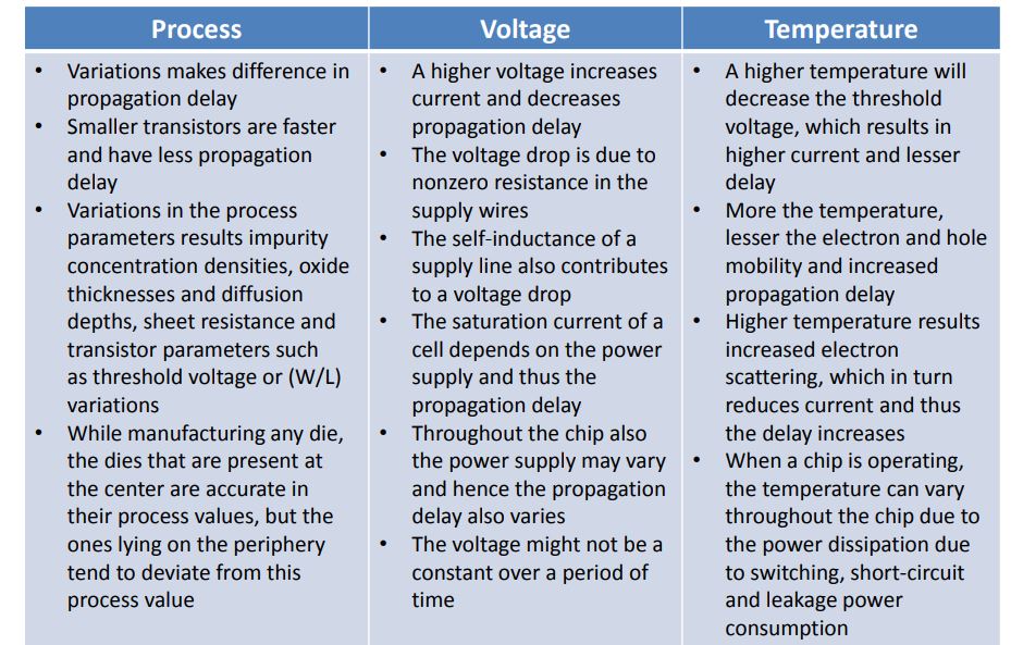
Corners are meant to capture variations in the manufacturing Process, along with expected variations in the Voltage and Temperature of the environment in which the chip will operate
Corners are independent on functional settings
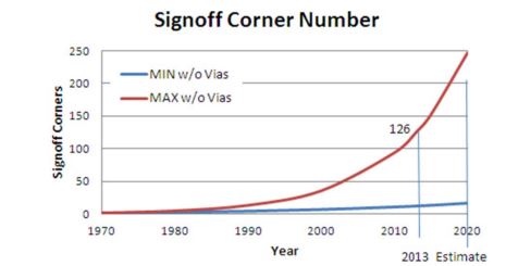
As technology shrinks, variations increases since smaller geometries have had a higher variability
As a result the number of Corners and Derates also grows
It is important to find minimum number of Corners, because run-time and Turn Around Time increases with increased number of Corners
E.g. run only slow metal at SS for Maximum Frequency
Also each Corner need its own OCV timing margins
The more Corners are used, the more pessimistic the timing signoff
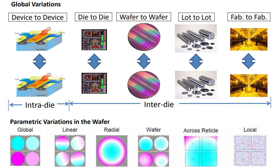
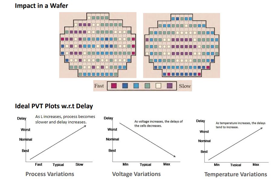
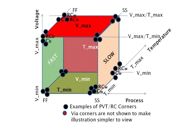
At each global Corner the Die experiences
External Voltage (like Minimum, Maximum, Typical)
Temperature (like Minimum, Typical, Maximum)
Process Shifts in (independent)
Transistors (Slow: SS, Typical: TT, Fast: FF or mixed SF & FS)
Interconnects (4 RC-extremes and RC-typical and Via Minimum, Maximum, Typical
Capacitance/ Resistance)
Vias are independent and not practically correlated with RC-wire models
Possible Vias models: VRCBEST, VCBEST, VRCWORST, VCWORST, VRCTYP Total number of Corners ={P: SS & FF & TT} x {V: Min. & Max. & Typ.} x {T: Min. & Max. & Typ.} x {RC: RCBEST, CBEST, RCWORST, CWORST, RCTYP}
E.g 3x3x3x5=135 PVT/RC Corners
By considering Aging Degradation two more corners will come in to picture Beginning-Of-Life (BOL) and End-Of-Life (EOL)
Even more Corners are needed for advanced nodes due to:
Temperature Inversion
Non-Linearity in Voltage
Designs with multi voltage domains
Additional voltages for over-and under-drive design modes
DPT (Double Patterning Technology) may add new corners
Via Capacitance Corners (additional to resistance corners) due to using wide Vias
Using FinFET and 3D structures may also contribute to Corner numbers and may decrease model accuracy
Using so many PVT/RC/Via corners will be not acceptable from the design time and costs considerations
Additionally, the number of Signoff Scenarios is a product of Corners and Modes (functional, test, etc.) and becomes too big to be handled by the tools
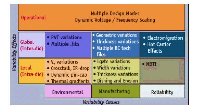
Need for Corner Analysis
PVT Variations
Corner Analysis
PVT/RC Corners
RC Corners
CBEST
It has minimum capacitance. So also known as CMIN corner
Interconnect Resistance is larger than the Typical corner
This corner results in smallest delay for paths with short nets and can be used for min-path-analysis
CWORST
Refers to corners which results maximum Capacitance. So also known as CMAX corner.
Interconnect resistance is smaller than at typical corner
This corners results in largest delay for paths with shorts nets and can be used for max-path-analysis
RC-BEST
Refers to the corners which minimize interconnect RC product. So also known as RC-MIN corner
Typically corresponds to smaller etch which increases the trace width. This results in smallest resistance but corresponds to larger than typical capacitance
Corner has smallest path delay for paths with long interconnects and can be used for min-path- analysis
RC-WORST
Refers to the corners which maximize interconnect RC product. So also known as RC-MAX corner
Typically corresponds to larger etch which reduces the trace width. This results in largest resistance but corresponds to smaller than typical capacitance
Corner has largest path delay for paths with long interconnects and can be used for max-path- analysis
Typical
This refers to nominal value of interconnect Resistance and Capacitance
Temperature Inversion
Temperature Inversion Dependence
A problem first described by Vassilios Gerousis of Infineon Technologies in 2003
Current, I = K . μ . ( VGS - VTH)2 ; where mobility (μ) and Threshold Voltage (VTH) are functions of Temperature
At high voltage μ determines the Drain current where as at lower voltages VTH determines the drain current
So at higher voltages device delay increase with temperature but at lower voltages, device delay decreases with temperature
At advanced Technology Nodes though the Threshold Voltage has not reduced much, but the Gate Overdrive Voltage has reduced due to the reduction of supply voltages
Therefore, Temperature Inversion Effects are more observed in Technology Nodes below 40nm
Cross Corner Analysis
Cross Corners
The consequence of Temperature Inversion is that the actual worst case for delay can occur at a temperature different from the highest temperature
E.g., as high-VT, low-leakage cells get colder they do not speed up in the way that circuits built around faster low-VT transistors do
The reason being that unlike the older technologies where Process, voltage, temperature (PVT) conditions are chosen with highest temperature to be the worst conditions for synthesis and P&R timing closure which is not true now
As a result the worst corner is not always easy to predict thus we need Cross Corners to identify the worst corner
The designers have to take into account the libraries corresponding to the lowest temperature PVT due to the temperature inversion effects
The Two Corner Analysis
Late (setup) analysis at weak, minimum voltage, high temperature conditions
Early (hold) analysis at strong, maximum voltage, low temperature conditions
Modes of Analysis
Modes
A Mode is defined as an operational setting of the chip
Mode is linked to a unique set of timing constraints
Mode can be associated with a set of corners to include only real combinations
Mode data is found in .sdc
Common Operational Modes
High-speed clocks mode
Slow clocks mode
Sleep mode
Debug mode
Scan capture mode
Scan shift mode
LBIST mode
JTAG mode
MBIST mode
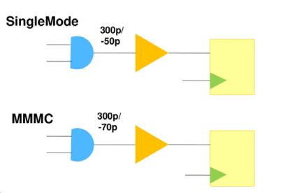
MC/MM Analysis
Scenarios
A severely limited Corner/Mode views that combines the worst-case parameters to run multiple extraction/timing analysis
Mode or Corner or a combination of both analyzed and optimized
E.g. Functional Mode - Slow Corner (func_setup_ss_0.9v_125c)
E.g. Logic BIST Mode - Fast Corner (lbist_hold_ff_1.1v_m40c)
Multi Corner (MC)/ Multi Mode (MM) Analysis (Multi-Scenario)
A technique intended to provide high confidence results for timing and other metrics without performing exhaustive simulation of all possible IC conditions
MCMM needed because of multiple dominant corners
MCMM eliminates the situation where a Hold fix in one mode can break the Setup in the other Modes
MCMM helps to avoid switching between different Corners/Modes to fix Setup/Hold violation
Avoids over fixing/ under fixing a Hold violation in a particular Corner
Reduces Hold buffer count
Reduce number of manual timing ECOs
Faster design closure
Helps in reducing the pessimistic margins and so is also called as Design-for-Variability (DFV)
Performed as concurrent analysis & optimization
Multi-corner analysis to examine the effects of process and environmental variations as well as changes caused by shifts into different operating modes
MCMM is the terminology by Synopsys & MMMC is the terminology by Cadence
OCV
On-Chip Variation (OCV) — On-chip variation (OCV) is a recognition of the intrinsic variability of semiconductor processes and their impact on factors such as logic timing
The number of contributors to timing variability has increased and led to significant variations not just between wafers but across individual wafers and increasingly intra-die
ICs from one batch of wafers being ‘slow’ or ‘fast’ relative to nominal estimates
Initially, timing analysis accounting for OCV was handled by telling the STA tool to apply a global margin (derate) across the entire chip using a percentage or delay estimate that the designer or the foundry considered safe
Timing variation was primarily a consequence of subtle shifts in manufacturing conditions that would lead to ICs from one batch of wafers being ‘slow’ or ‘fast’
OCV provides a single derating factor for all instances, so the results can be grossly optimistic or pessimistic
So OCV may led to performance degradation while closing the timing
OCV handles global variations with Corners (best case, nominal, and worst-case combinations)
The biggest challenge in OCV variations is handling the local uncorrelated variables
OCV Derating
Derating
Derating is a way to model slow and fast signals in On-Chip-Variation (OCV)
It is an extra pessimism added in Static Timing Analysis, in order to account for the On-Chip Variation effects
10% derate in simple terms means, over designing the timing by 10%
So that chip will work at the desired frequency, even if there is a variation effect across the die
Scaling factors can be set independently for data paths, clock paths, cell delays, net delays, and cell timing checks
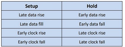
Early and late derates applied to launch paths and capture paths depending upon Setup/Hold Analysis
Maximum and minimum derating means to multiply the original timing library delay values by the derate value
Derating decreases as process matures
E.g. For 65nm designs at earlier days 15% derates added but now a days only 5% derates need to be added
OCV Timing Checks
Scaling factors can be set independently for data paths, clock paths, cell delays, net delays and cell timing checks
Early and late derates applied to Launch Paths and Capture Paths depending upon Setup/Hold Analysis
Setup Check with OCV
Maximum possible data arrival is determined by taking the maximum delays along the clock path to the start-point register and the maximum delays along the slowest data path from the start-point register to the endpoint register
The earliest possible clock arrival at the end-point register is determined by taking the minimum delays along the clock path to the end-point register
Hold Check with OCV
For hold check, we use min delays for the clock path to the start-point register, min delays through the shortest data path, and max delays for the clock path to the end-point register
OCV Enhancements
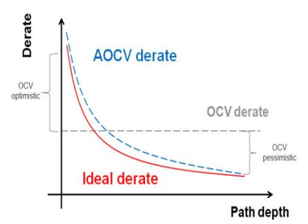
Advanced OCV (AOCV)
Uses context-specific derating instead of a single global derate value
Reduce design margins and lead to fewer timing violations
Determines derate values as a function of logic depth and relative cell or net location
As a function of cell depth it gives less pessimistic margins to the path
Corrects pessimism and optimism in timing derate by accurately modeling variance
Sometimes referred to as Location-based OCV or Stage based OCV
Stage based OCV is a systematic correction to liberty timing models for on chip variation based on the logic depth of a path
Logic depth and location based approach deals based approach with systematic effects
Advanced OCV computes the length of the diagonal of the bounding box that contains the cells being analyzed to select an appropriate derate value from the table constructed by test-chip results
Global variations cancel out over long distances
For data path derate is a measure of statistical delay/ Corner delay
For clock path derate is a measure of slew
Advanced OCV (AOCV)
AOCV table generation is independent of the methodology
AOCV table can be easily adapted to tools and is companion to .lib
AOCV tables have derate values for each cell for different depths (path length)
AOCV Derates are defined by analyzing the ratio of delay at the global corner with local variance to a fixed corner
AOCV defines 8 derate values for each cell at each depth
Statistical OCV (SSTA modeling)
Statistical OCV (SOCV) is a simplified approach to SSTA that uses a single local variable as Derate
It is also referred as Parametric OCV (POCV)
It takes elements of SSTA and implementing them in a way that is less compute-intensive
It solves the major limitations of AOCV, including variation dependency on slew and load and the assumption that the same cell, or load, is in the path
It combines delay variations in Cells, Wires and Vias
It promises near SSTA accuracy for a small additional cost of runtime and memory compared to AOCV
It can include signoff-accurate signal integrity (SI) analysis
Handles DPT and some other dynamic effects in a conservative static way
It ignores correlations and number of timing paths
SOCV is much more accurate than AOCV, especially for graph-based analysis
SOCV can be validated with SPICE Monte Carlo Analysis
CRPR/ CPPR
Common Path Pessimism (CPP)
Applying different derating for the Launch and Capture Clock is overly pessimistic
The Clock Tree will be at only one PVT condition, either as a maximum path or as a minimum path (or anything in between) but never both at the same time
CPP is the delay difference along the common portion of the Clock Tree due to different deratings for Launch and Capture Clock Paths
Pessimism caused by different derating factors applied on the common part of the Clock Tree is called Common Path Pessimism (CPP)/ Clock Re-convergence Pessimism (CRP) which should be removed during the analysis
CRP or CPP = (maximum clock delay or skew) - (minimum clock delay or skew)
Common Path Pessimism Removal (CPPR) or Clock Reconvergence Pessimism Removal (CRPR)
Both CPPR and CRPR are removal of artificially introduced pessimism between the Launch Clock Path and the Capture Clock Path in timing analysis