FloorPlan

FloorPlan


Before starting with the floorplan we will perform import design, sanity checks and partitioning.

Import Design

— The following input files information are loaded to the PnR tool
  • Netlist (.v/ .vhd/ .edif)
  • Physical Libraries (.lef)
  • Timing Libraries (.lib)
  • Technology Files
  • Constraints (.sdc)
  • IO Info. File (optional)
  • Power Spec. File (optional)
  • Optimization Directives (optional)
  • Clock Tree Spec. File (optional at floorplan stage)
  • DEF/ FP (optional if floorplan is not done)
— Core area is approximately calculated by the tool from the Netlist

— While Importing, first we have to load the LEF files and then LIB files

Sanity Checks

— Sanity Checks mainly checks the quality of netlist in terms of timing.
— It also consists of checking the issues related to Library files, Timing Constraints, IOs and Optimization Directives

1. Library checks
    • Missing cell information
    • Missing pin information
    • Duplicate cells

2. Design checks
    • Inputs with floating pins
    • Nets with tri-state drivers
    • Nets with multiple drivers
    • Combinational loops
    • Empty modules
    • Assign statements

3. Constraint checks
    • All flops are clocked or not
    • There should not be unconstraint paths
    • Input and output delays

Partitioning

Physical Design Netlist
  • All Ports must be defined and should be present
  • No Assignment Statements (1’b0 or 1’b1 statements): Assignment statements causes feed-through (i/p directly to o/p) and can be avoided by adding buffers
  • No Unmapped Cells
  • No Combinational Timing Loops

Styles of Implementation

Flat
  • Small to Medium ASIC
  • Better Area Usage Since no reserve space around each sub-design for power/ground
Hierarchical
  • For very large design
  • When sub-systems are design individually
  • Possible only if a design hierarchy exist
- The Hierarchical Partitioning is done prior to Floorplan
- Partition can be done based on
  • Design Hierarchy
  • Timing Criticality
  • Functionality
  • Clock Domain
  • Design Files
  • Block Size
     partitioning in physical design
- Partitioning Inputs and Outputs by Registers
- Minimize Cross-Partition-Boundary IO
- For Sub-block designs, the Partitioning is not required
- For Full Chip only we need to design with Partitioning

FloorPlanning

Floorplan is one the critical & important step in Physical design. Quality of your Chip / Design implementation depends on how good is the Floorplan. A good floorplan can be make implementation process (place, cts, route & timing closure) cake walk. On similar lines a bad floorplan can create all kind issues in the design (congestion, timing, noise, IR, routing issues). A bad floorplan will blow up the area, power & affects reliability, life of the IC and also it can increase overall IC cost (more effort to closure, more LVTs/ULVTs).

Objectives of Floorplan

  • minimize the area
  • minimize the Timing
  • Reduce the wire length
  • Making routing easy
  • Reduce IR drop

Inputs of Floorplan

  • Technology file (.tf)
  • Netlist
  • SDC
  • Library files (.lib & .lef) & TLU+ file

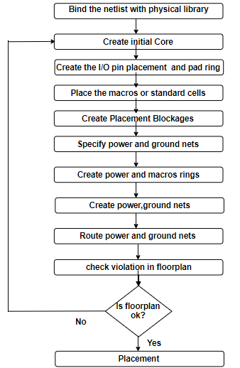
Floorplan Flowchart

            floorplan flowchart

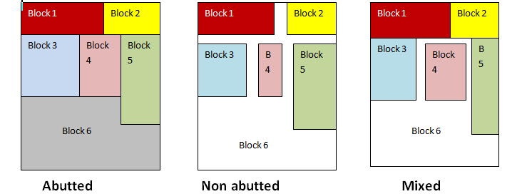
Types of Floorplan Techniques

  • Abutted floorplan : Channel less placement of blocks.
  • Non-Abutted Floorplan : Channel based placement of blocks.
  • Mix of both: partially abutted with some channels.

    floorplan types, abutted non abutted and mix

Terminologies and Definitions

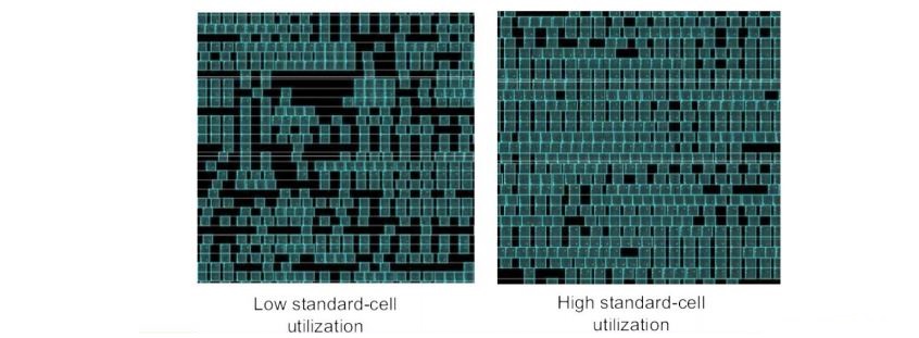
Utilization
  • Area of the core that is used by placed Standard Cells and Macros expressed inpercentage
Manufacturing Grid
  • The smallest geometry that semiconductor foundry can process or smallest resolution of your technology process (e.g. 0.005)
  • All drawn geometries during Physical Design must snap to this grid
  • While Masking fab. use this as reference lines
Standard Cell Site/ Standard Cell Placement Tile/ Unit Tile
  • The minimum Width and Height a Cell that can occupy in the design
  • The Standard Cell Site will have the same height as Standard Cells, but the width will be as small as your smallest Filler Cell
  • It’s one Vertical Routing Track and the Standard Cell Height
  • All Standard Cells must be multiple of Unit Tile
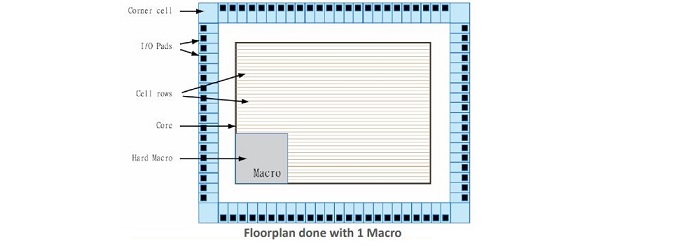
Standard Cell Rows
  • Rows are actually the Standard Cell Sites abut side by side and then Standard Cells are placed on these Rows
  • Cells with the equal no. of Track definition will have same height
Placement Grid
  • Placement Grid is made up of Standard Cell Site
  • Its always a multiple of Manufacturing Grid
  • Placement Grid is made up of the Rows which are composed of Sites
Routing Grid and Routing Track
  • Horizontal and Vertical line drawn on the layout area which will guide for making interconnections
  • The Routing Grid is made up of the Routing Tracks
  • Routing Tracks can be Grid-based, Gridless based or Subgrid-based
Flight-line/ Fly-line
  • Virtual connection between Macros and Macro or Macros and IOs
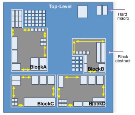
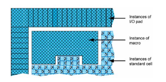
Macro
  • Any instances other than Standard Cell and is as loaded as black box to the design is Macro
  • Intellectual Property (IP) e.g. RAM, ROM, PLL, Analog Designs etc.
  • Hard Macro: IP with Layout implemented
  • Soft Macro: IP without Layout implemented (HDL)

Steps in Floorplan

  • Initialize with Chip & Core Aspect Ratio (AR)
  • Initialize with Core Utilization
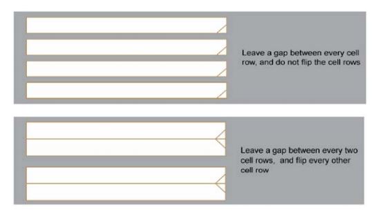
  • Initialize Row Configuration & Cell Orientation
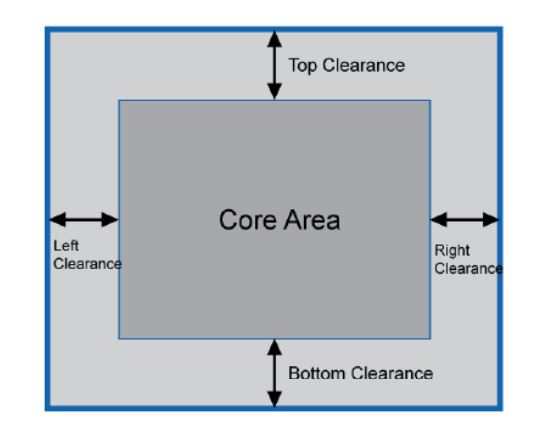
  • Provide the Core to Pad/ IO spacing (Core to IO clearance)
  • Pins/ Pads Placement
  • Macro Placement by Fly-line Analysis
  • Macro Placement requirements are also need to consider
  • Blockage Management (Placement/ Routing)

Utilization

Row Configuration

  • Slanting lines in the side of the cell rows denote the Cell Orientation utilization in floorplan, physicaldesign utilization in floorplan, physicaldesign
         Butt and flip is Most common because of better space utilization

Core to Pad/ IO spacing

  • Core to IO clearance
  • Used for Placing IOs and Power Ring
       core to io spacing in floorplan

io spaching in floorplan

  • or simply Height/Width
  • Aspect Ratio decides the shape
  • Full chip Aspect Ratio can have a maximum value of 1.25
ratio is floorplan, physical design

IO Placement

  • Chip Level its IO Pads and Block Level its IO Pins
  • Pin is a logical entity and is a property of a Port
  • Port is a physical entity and a Port have only 1 Pin associated with it
  • Netlist will have Pins and Layout will have Ports
  • Unplaced Port is not represented in the Layout
            io placement in physical ddesign
  • Different types of IOs
  • Signal Pads/Pins
  • Core Power Pads/Pins
  • IO Power Pads/Pins
  • Corner Pads (Doesn’t hold any logic, provides IO Pad Ring connectivity)
  • Filler Pads (Fill the gaps between IO pads to get the Ring Connectivity)
  • Physical-only pads that are not part of the input Gate level Netlist need to be inserted prior to reading IO constraints
  • IO Pads enables the design to operate at different voltages with the help of Level Shifters, Pre-Drivers (at Core Voltage)Post-Drivers (at IO Voltage)
  • No of Core Power Pads needed:         core power pads in physical design
  • There will be 1 Core GND Pad along with every Core Power Pad
  • No. of IO Power Pads needed:
           Thumb Rule: 1 pair of IO power pads for every 4 to 6 signal pads.


Macro Placement

macro placement is done based on connectivity information of macro to IO cell and macro to macro. macro placement is very critical for congestion and timing. macro placement should result in uniform std cell area.

  • Fly-line Analysis (For Connectivity information)
  • Macro keep-out (For Uniform Standard Cell Region)
  • Channel Calculation (Critical for Congestion and Timing)
  • Avoid odd shaped area for Standard Cells
  • Funnel shaped Macro Placements are preferred
  • Fix the Macro locations, so that tool wont alter during Optimization
  • Spacing between Macro:
macro placement, floorplanning, physical design

Macro Placement Tips

  • Place macros around chip periphery, so that core area will be clustered
  • Consider connections to fixed cells when placing Macros
  • In advanced Technology Nodes Macro Orientation is fixed since the Poly Orientation can’t vary, so there will be restrictions in Macro Orientation
  • Reserve enough room around Macros for IO Routing
  • Reduce open fields as much as possible
  • Provide necessary Blockages around the Macro macro placement, floorplanning, physical design

Blockages

  • blockages are specific location where placing of cells are blocked.
  • blockages acts like guidelines for placement of std cells.
  • blockages will not be guiding the tool to place the std cells at some particular area, but it won't allow the tool to place the std cell in the blocked area.
    blockages in physical design

Placement Blockage & Routing Blockage
  • Both of the Blockages can again be classified as-
    • Hard, Soft and Partial Blockages

  • Hard Blockage
    • Complete Standard Cell Blockage
    • std cell blockages are mostly used to
      • avoid routing congestion at macro corners
      • Restrict std cells to certain regions in the design
      • control power rail generation at macro cells
  • Soft Blockage
    • Non-Buffering Blockage, only buffers can be placed and std cells cannot be placed
  • Partial Blockage
    • Partial Standard Cell Blockage and is used to avoid congestion
    • We can Block Standard Cells as per the required percentage value

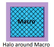
Keep-out / Halo

                             keepout margin, halo in physical design

  • Halo is similar to Soft Blockage meaning it allows placement of buffers and inverters in its area. (Terminology in Cadence EDI)
  • Its basically a keep-out Macro margin
  • Halo respects Macro while other Blockages respect location
                 i.e., even if Macro is moved Halo also moves along with it
  • Halos of adjacent macros can overlap.

Issues arises due to bad Floorplan

  • Congestion near Macro Pins/ Corners due to insufficient Placement Blockage
  • Std. Cell placement in narrow channels led to Congestion
  • Macros of same partition which are placed far apart can cause Timing Violation

    floorplanning, physical design

Floorplan Qualification:

  • No I/O ports short
  • All I/O ports should be placed in routing grid
  • All macros in placement grid
  • No macros overlapping
  • Check PG connections (For macros & pre-placed cells only)
  • All the macros should be placed at the boundary
  • There should not be any notches. If unavoidable, proper blockages has to be added
  • Remove all unnecessary placement blockages & routing blockages (which might be put during floor-plan & pre-placing)

Floorplan outputs

  • IO ports placed
  • cell rows created
  • macro placement final
  • core boundary and area
  • pin position
  • floorplan def
  • What is synthesis?
  • Goals of synthesis
  • Synthesis Flow
  • Synthesis (input & output)
  • HDL file gen. & lib setup
  • Reading files
  • Design envi. Constraints
  • Compile
  • Generate Reports
  • Write files
Go To page
  • Netlist(.v or .vhd)
  • Constraints
  • Liberty Timing File(.lib or .db)
  • Library Exchange Format(LEF)
  • Technology Related files
  • TLU+ File
  • Milkyway Library
  • Power Specification File
  • Optimization Directives
  • Design Exchange Formats
  • Clock Tree Constraints/ Specification
  • IO Information File
Go To page
  • import design
  • sanity checks
  • partitioning (flat and hierarchy)
  • objectives of floorplan
  • Inputs of floorplan
  • Floorplan flowchart
  • Floorplan Techniques
  • Terminologies and definitions
  • Steps in FloorPlan
  • Utilization
  • IO Placement
  • Macro Placement
  • Macro Placement Tips
  • Blockages (soft,hard,partial)
  • Halo/keepout margin
  • Issues arises due to bad floor-plan)
  • FloorPlan Qualifications
  • FloorPlan Output
Go To page
  • levels of power distribution
  • Power Management
  • Powerplanning involves
  • Inputs of powerplan
  • Properties of ideal powerplan
  • Power Information
  • PowerPlan calculations
  • Sub-Block configuration
  • fullchip configuration
  • UPF Content
  • Isolation Cell
  • Level Shifters
  • Retention Registers
  • Power Switches
  • Types of Power dissipation
  • IR Drop
  • Electromigration
Go To page
  • Pre-Placement
  • Pre-Placement Optimization
  • Placement
  • Placement Objectives
  • Goals of Placement
  • Inputs of Placement
  • Checks Before placement
  • Placement Methods(Timing & Congestion)
  • Placement Steps
  • Placement Optimization
  • Placement Qualifications
  • Placement Outputs
Go To page
  • Pre-CTS Optimization
  • CTS
  • Diff b/w HFNS & CTS
  • Diff b/w Clock & normal buffer
  • CTS inputs
  • CTS Goals
  • Clock latency
  • Clock problems
  • Main concerns for Clock design
  • Clock Skew
  • Clock Jitter
  • CTS Pre requisites
  • CTS Objects
  • CTS Flow
  • Clock Tree Reference
  • Clock Tree Exceptions
  • CTS Algorithm
  • Analyze the Clock tree
  • Post CTS Optimization
  • CTS Outputs
Go To page
  • Importance of Routing as Technology Shrinks
  • Routing Objectives
  • Routing
  • Routing Inputs
  • Routing Goals
  • Routing constraints
  • Routing Flow
  • Trial/Global Routing
  • Track Assignment
  • Detail/Nano Routing
  • Grid based Routing
  • Routing Preferences
  • Post Routing Optimization
  • Filler Cell Insertion
  • Metal Fill
  • Spare Cells Tie-up/ Tie-down
Go To page
  • Diff b/w DTA & STA
  • Static Timing Analysis
  • main steps in STA
  • STA(input & output)
  • Timing Report
  • Clocked storage elements
  • Delays
  • Pins related to clock
  • Timing Arc
  • Timing Unate
  • Clock definitions in STA
  • Timing Paths
  • Timing Path Groups
  • Clock Latency
  • Insertion Delay
  • Clock Uncertainty
  • Clock Skew
  • Clock Jitter
  • Glitch
  • Pulse width
  • Duty Cycle
  • Transition/Slew
  • Asynchronous Path
  • Critical Path
  • Shortest Path
  • Clock Gating Path
  • Launch path
  • Arrival Path
  • Required Time
  • Common Path Pessimism(CPP/CRPR)
  • Slack
  • Setup and Hold time
  • Setup & hold time violations
  • Recovery Time
  • Removal Time
  • Recovery & Removal time violations
  • Single Cycle path
  • Multi Cycle Path
  • Half Cycle Path
  • False Path
  • Clock Domain Crossing(CDC)
  • Clock Domain Synchronization Scheme
  • Bottleneck Analysis
  • Multi-VT Cells(HVT LVT SVT)
  • Time Borrowing/Stealing
  • Types of STA (PBA GBA)
  • Diff b/w PBA & GBA
  • Block based STA & Path based STA
Go To page

  • Congestion Analysis
  • Routing Congestion Analysis
  • Placement Cong. Analysis
  • Routing Congestion causes
  • Congestion Fixes
  • Global & local cong.
  • Congestion Profiles
Go To page
  • Power Analysis
  • Leakeage Power
  • Switching Power
  • Short Circuit
  • Leakage/static Power
  • Static power Dissipation
  • Types of Static Leakage
  • Static Power Reduction Techniques
  • Dynamic/Switching Power
  • Dynamic Power calculation depends on
  • Types of Dynamic Power
  • Dynamic Power Reduction Techniques
Go To page
  • IR Drop Analysis
  • Types of IR Drop & their methodologies
  • IR Drop Reasons
  • IR Drop Robustness Checks
  • IR Drop Impacts
  • IR Drop Remedies
  • Ldi/dt Effects
Go To page

  • Design Parasitics
  • Latch-Up
  • Electrostatic Discharge(ESD)
  • Electromigration
  • Antenna Effect
  • Crosstalk
  • Soft Errors
  • Sef Heating
Go To page
  • Cells in PD
  • Standard Cells
  • ICG Cells
  • Well Taps
  • End Caps
  • Filler Cells
  • Decap Cells
  • ESD Clamp
  • Spare Cells
  • Tie Cells
  • Delay Cells
  • Metrology Cells
Go To page
  • IO Pads
  • Types of IO Pads
Go To page
  • Delay Calculation
  • Delay Models
  • Interconnect Delay Models
  • Cell Delay Models
Go To page
  • Engineering Change Order
  • Post Synthesis ECO
  • Post Route ECO
  • Post Silicon ECO
  • Metal Layer ECO Example
Go To page
  • std cell library types
  • Classification wrt density and Vth
Go To page

  • The Discontinuity
  • Discontinuity: Classification
  • DFM/DFY
  • Yield Classification
  • Why DFM/DFY?
  • DFM/DFY Solution
  • Wire Spreading
  • metal Fill
  • CAA
  • CMP Aware-Design
  • Redundant Via
  • RET
  • Litho Process Check(LPC)
  • Layout Dependent Effects
  • Resolution Enhancement Techniques
  • Types of RET
  • Optical Proximity Correction(OPC)
  • Scattering Bars
  • Multiple Patterning
  • Phase-shift Masking
  • Off-Axis Illumination
Go To page
  • Corners
  • Need for corner analysis
  • PVT Variations
  • Corner Analysis
  • PVT/RC Corners
  • Temperature Inversion
  • Cross Corner Analysis
  • Modes of Analysis
  • MC/MM Analysis
  • OCV
  • Derating
  • OCV Timing Checks
  • OCV Enhancements
  • AOCV
  • SSTA
  • CRPR/CPPR
Go To page
Copyright © 2021