
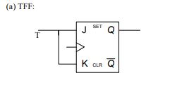
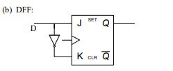
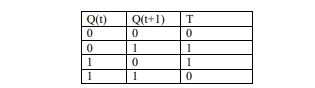
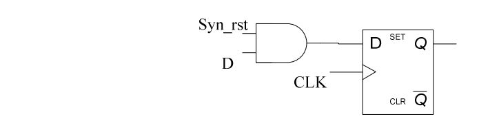
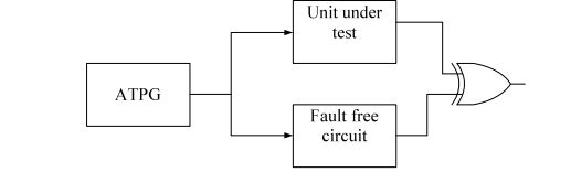
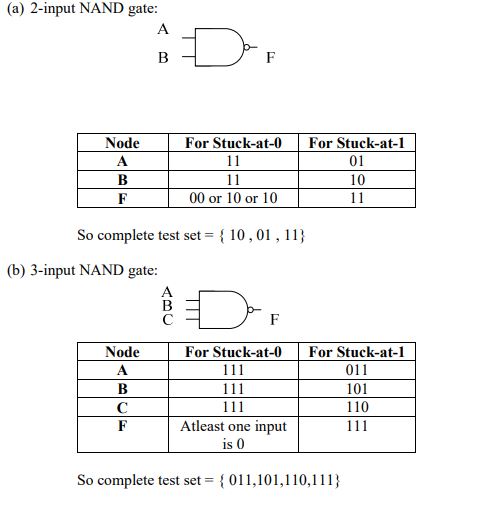
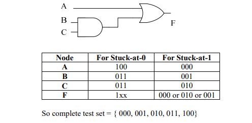
Topics


 .
.
 .
.


- What is synthesis?
- Goals of synthesis
- Synthesis Flow
- Synthesis (input & output)
- HDL file gen. & lib setup
- Reading files
- Design envi. Constraints
- Compile
- Generate Reports
- Write files
- Netlist(.v or .vhd)
- Constraints
- Liberty Timing File(.lib or .db)
- Library Exchange Format(LEF)
- Technology Related files
- TLU+ File
- Milkyway Library
- Power Specification File
- Optimization Directives
- Design Exchange Formats
- Clock Tree Constraints/ Specification
- IO Information File
- import design
- sanity checks
- partitioning (flat and hierarchy)
- objectives of floorplan
- Inputs of floorplan
- Floorplan flowchart
- Floorplan Techniques
- Terminologies and definitions
- Steps in FloorPlan
- Utilization
- IO Placement
- Macro Placement
- Macro Placement Tips
- Blockages (soft,hard,partial)
- Halo/keepout margin
- Issues arises due to bad floor-plan)
- FloorPlan Qualifications
- FloorPlan Output
- levels of power distribution
- Power Management
- Powerplanning involves
- Inputs of powerplan
- Properties of ideal powerplan
- Power Information
- PowerPlan calculations
- Sub-Block configuration
- fullchip configuration
- UPF Content
- Isolation Cell
- Level Shifters
- Retention Registers
- Power Switches
- Types of Power dissipation
- IR Drop
- Electromigration
- Pre-Placement
- Pre-Placement Optimization
- Placement
- Placement Objectives
- Goals of Placement
- Inputs of Placement
- Checks Before placement
- Placement Methods(Timing & Congestion)
- Placement Steps
- Placement Optimization
- Placement Qualifications
- Placement Outputs
- Pre-CTS Optimization
- CTS
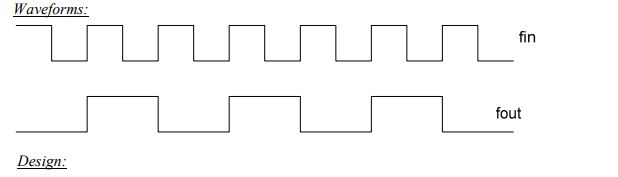
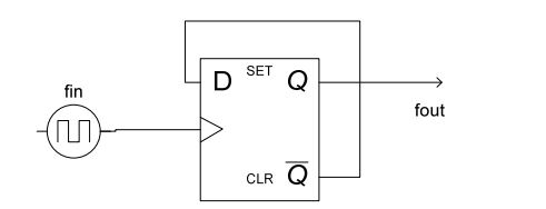
- Diff b/w HFNS & CTS
- Diff b/w Clock & normal buffer
- CTS inputs
- CTS Goals
- Clock latency
- Clock problems
- Main concerns for Clock design
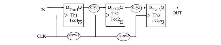
- Clock Skew
- Clock Jitter
- CTS Pre requisites
- CTS Objects
- CTS Flow
- Clock Tree Reference
- Clock Tree Exceptions
- CTS Algorithm
- Analyze the Clock tree
- Post CTS Optimization
- CTS Outputs
- Importance of Routing as Technology Shrinks
- Routing Objectives
- Routing
- Routing Inputs
- Routing Goals
- Routing constraints
- Routing Flow
- Trial/Global Routing
- Track Assignment
- Detail/Nano Routing
- Grid based Routing
- Routing Preferences
- Post Routing Optimization
- Filler Cell Insertion
- Metal Fill
- Spare Cells Tie-up/ Tie-down
- Diff b/w DTA & STA
- Static Timing Analysis
- main steps in STA
- STA(input & output)
- Timing Report
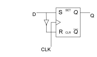
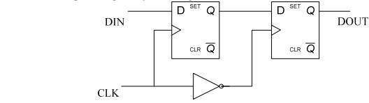
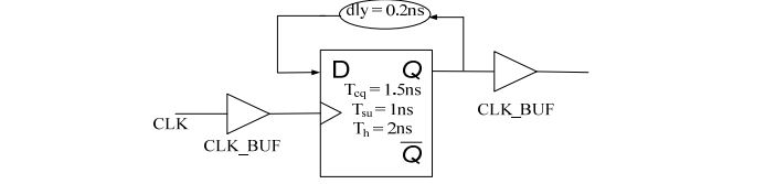
- Clocked storage elements
- Delays
- Pins related to clock
- Timing Arc
- Timing Unate
- Clock definitions in STA
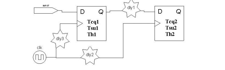
- Timing Paths
- Timing Path Groups
- Clock Latency
- Insertion Delay
- Clock Uncertainty
- Clock Skew
- Clock Jitter
- Glitch
- Pulse width
- Duty Cycle
- Transition/Slew
- Asynchronous Path
- Critical Path
- Shortest Path
- Clock Gating Path
- Launch path
- Arrival Path
- Required Time
- Common Path Pessimism(CPP/CRPR)
- Slack
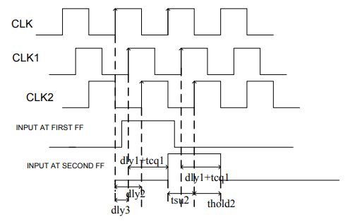
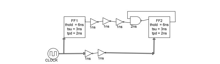
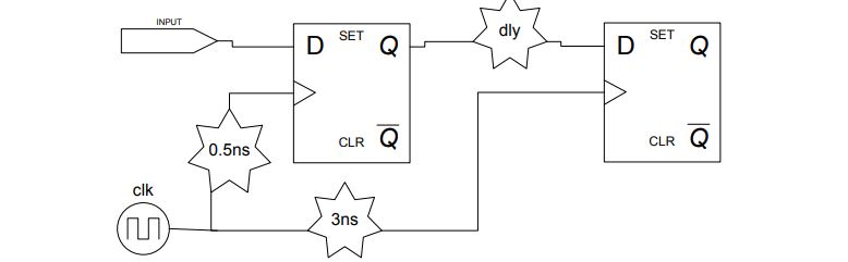
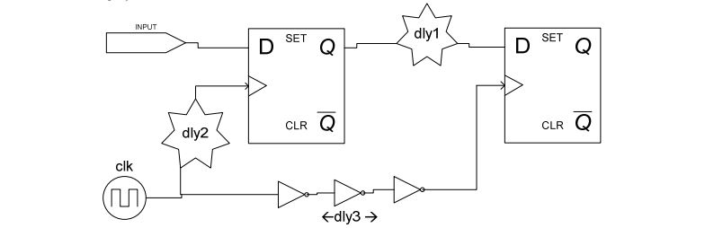
- Setup and Hold time
- Setup & hold time violations
- Recovery Time
- Removal Time
- Recovery & Removal time violations
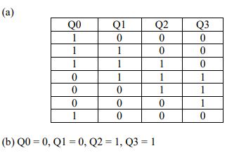
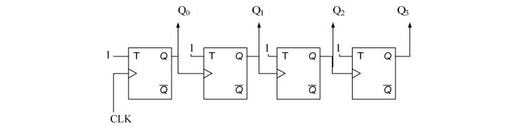
- Single Cycle path
- Multi Cycle Path
- Half Cycle Path
- False Path
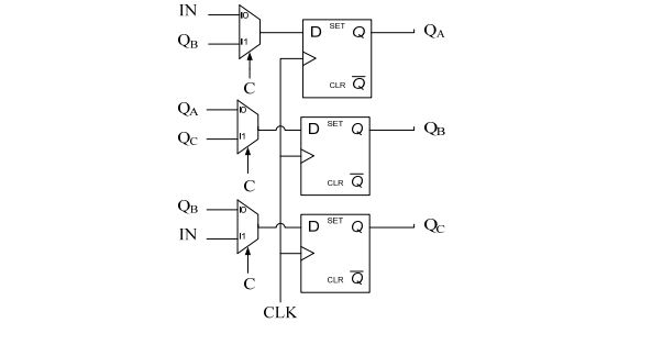
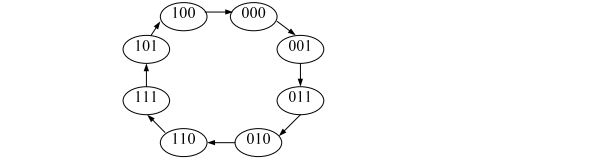
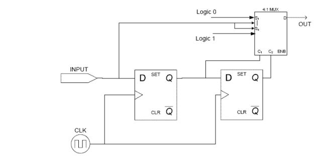
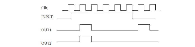
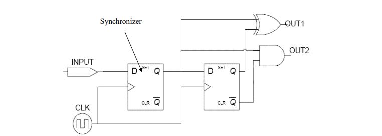
- Clock Domain Crossing(CDC)
- Clock Domain Synchronization Scheme
- Bottleneck Analysis
- Multi-VT Cells(HVT LVT SVT)
- Time Borrowing/Stealing
- Types of STA (PBA GBA)
- Diff b/w PBA & GBA
- Block based STA & Path based STA
- Congestion Analysis
- Routing Congestion Analysis
- Placement Cong. Analysis
- Routing Congestion causes
- Congestion Fixes
- Global & local cong.
- Congestion Profiles
- Power Analysis
- Leakeage Power
- Switching Power
- Short Circuit
- Leakage/static Power
- Static power Dissipation
- Types of Static Leakage
- Static Power Reduction Techniques
- Dynamic/Switching Power
- Dynamic Power calculation depends on
- Types of Dynamic Power
- Dynamic Power Reduction Techniques
- IR Drop Analysis
- Types of IR Drop & their methodologies
- IR Drop Reasons
- IR Drop Robustness Checks
- IR Drop Impacts
- IR Drop Remedies
- Ldi/dt Effects
- Design Parasitics
- Latch-Up
- Electrostatic Discharge(ESD)
- Electromigration
- Antenna Effect
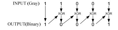
- Crosstalk
- Soft Errors
- Sef Heating
- Cells in PD
- Standard Cells
- ICG Cells
- Well Taps
- End Caps
- Filler Cells
- Decap Cells
- ESD Clamp
- Spare Cells
- Tie Cells
- Delay Cells
- Metrology Cells
- IO Pads
- Types of IO Pads
- Delay Calculation
- Delay Models
- Interconnect Delay Models
- Cell Delay Models
- Engineering Change Order
- Post Synthesis ECO
- Post Route ECO
- Post Silicon ECO
- Metal Layer ECO Example
- std cell library types
- Classification wrt density and Vth
- The Discontinuity
- Discontinuity: Classification
- DFM/DFY
- Yield Classification
- Why DFM/DFY?
- DFM/DFY Solution
- Wire Spreading
- metal Fill
- CAA
- CMP Aware-Design
- Redundant Via
- RET
- Litho Process Check(LPC)
- Layout Dependent Effects
- Resolution Enhancement Techniques
- Types of RET
- Optical Proximity Correction(OPC)
- Scattering Bars
- Multiple Patterning
- Phase-shift Masking
- Off-Axis Illumination
- Corners
- Need for corner analysis
- PVT Variations
- Corner Analysis
- PVT/RC Corners
- Temperature Inversion
- Cross Corner Analysis
- Modes of Analysis
- MC/MM Analysis
- OCV
- Derating
- OCV Timing Checks
- OCV Enhancements
- AOCV
- SSTA
- CRPR/CPPR
