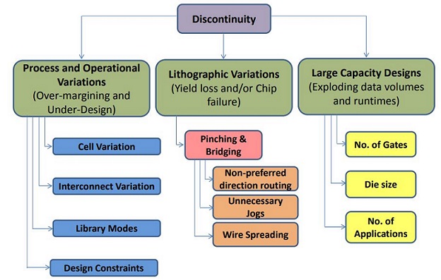
With each new Technology node, previously manageable challenges in physical implementation emerge as extremely disruptive discontinuities
At 180nm, timing closure was a disruptive challenge, which led to new physical synthesis technology
At 130nm, Signal Integrity (SI) closure was the main discontinuity
The new generation of challenges started at 65nm, are in full force at 45nm
The challenges will get worse as ICs venture into more advanced Technology nodes like 22/14nm
Designers are working at these Technologies to fully understand the new discontinuities
Special design enhancements are introduced under the title Design-forManufacturability (DFM) and Design-for-Yield (DFY) to overcome these Discontinuities
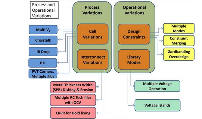
Discontinuity: Classification
DFM/DFY
Design for Manufacturability (DFM)/ Design for Yield (DFY)
Techniques to ensure the design can manufacture successfully with high yield
To ensures survival of the design, during the complex fabrication process
Lithography, etch, Chemical Mechanical Polishing (CMP), and mask systematic manufacturing variations surpass random variations as the prime limiters to catastrophic and parametric yield loss
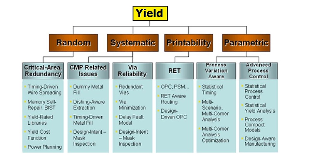
Yield
Percentage of manufactured products that meet all performance and functionality Specifications
The number of die that work as a percentage of the total number of die on the silicon wafer Yield = Good Chips/ Total Chips Measured Yield = Good Parts + Test Escapes − False Rejects/ All Parts
Memory fails more than logic, so repairable memory can improve Yield
DFY predicts chip yield at two points of the manufacturing flow wafer probe and during final test of the packaged chip and identifies what defects result in yield loss
Yield Classification
Why DFM/DFY ?
Need for DFM/DFY
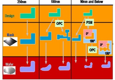
Current Lithographic techniques (193nm Laser) cannot print deep-submicron technology patterns without distortion
Higher design complexity and shrinking device geometries
More devices per unit area on a chip (device density)
Importance of DFM/DFY
Impact of variations, if not addressed in the design, will cause manufacturing issues, such as poor yields, long yield ramp-up times and poor reliability
The chips may completely miss the market window or may hit the market window but not economically viable
The chips may still function, but not at the required/expected speed
The chips appear to be reliable after volume production, but may suffer catastrophic failures in the field earlier than their expected life-cycle
DFM/DFY Solutions
DFM: Recommendations
Wire Spreading
The wire distribution spreads wires that are on the same metal layer as well as across different metal layers
The benefits gained from lower routing density are in improved manufacturing yield, reduced crosstalk noise, crosstalk delay and random particle defects
Metal Fill
Dummy metal fill
Timing aware metal fill
Unbalanced metal density across a chip may cause yield loss, so fill the empty spaces in the design with metal wires to meet the metal density rules required by most fabrication processes
Improved surface planarity helps decrease manufacturing variations that contribute to timing variability
Hot Spots and Critical Area Analysis (CAA)
Hot Spot/ Critical Area is the region at the center of a random defect which will cause circuit failure (yield loss)
By analyzing the critical areas, defect-limited yield can be estimated based on the probability of the failures of vias and point defects on routing
The larger the defect size, the larger the Critical Area
Critical area reduction improves yield
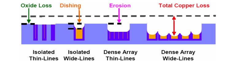
Chemical-Mechanical Polishing (CMP) is a technique for surface smoothing and material removal process to get globally planar wafer surface
Simultaneous polishing of copper, dielectric and barrier
Combination of chemical and mechanical interactions
The chemical effect by pH regulators, oxidizers or stabilizers
The mechanical action by submicron sized abrasive particles contained in the slurry flow between the polishing pad and the wafer surface
Dishing
Difference between the height of the copper in the trench and the height of the dielectric surrounding the copper trench
Copper dishing is higher for wider copper line or the spacing
It can thin the wire or pad, causing higher-resistance wires or lower reliability bond pads
Erosion
Difference between the dielectric thickness before CMP and after CMP
Dielectric erosion is higher for higher density
Erosion can result in a sub-planar dip on the wafer surface, causing short-circuits between adjacent wires on next layer
On-Chip Variation (OCV) from the interconnect thickness variation due to CMP becomes relatively larger and needs to be taken into consideration in the postlayout RC extraction and timing flow
Solution to CMP is CMP hotspot detection and fixing
CMP aware-design
Various degrees of Copper Dishing and Dielectric Erosion occur at different densities and metal line widths
In advanced nodes minimal material removal with atomically flat and clean surface finish has to be achieved
CMP is influenced by line width and pattern density
The dishing and erosion increase slowly as a function of increasing density and go into saturation when the density is more than 0.7
Oxide erosion and copper dishing can be controlled by area filling and metal slotting
Redundant Via
Redundant Vias use two, or more, Vias to connect the upper and lower routing layers together
Replacing single Vias with redundant (or double) Vias on signal nets improves reliability and reduce yield loss, due to via failures
Critical Area Analysis (CAA) identifies the requirement of Redundant Vias
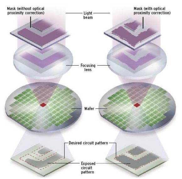
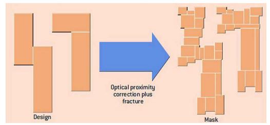
Resolution Enhancement Techniques (RET)
RET are methods used to modify photo-masks to compensate for limitations in the lithographic processes used to manufacture the chips
Have significantly increased the cost and complexity of sub-micron nanometer photomasks
The photomask layout is no longer an exact replica of the design layout
As a result, reliably verifying RET synthesis accuracy, structural integrity, and conformance to mask fabrication rules are crucial for the manufacture of nanometer regime VLSI designs
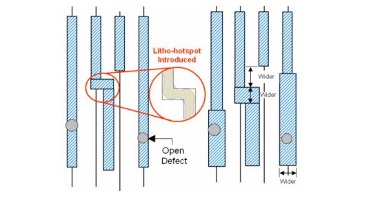
Litho Process Check (LPC)
Problem: Some DRC clean layouts do not print on silicon
Solution: Must-have litho hotspot detection and fixing of design
Layout Dependent Effects
Well Proximity Effect (WPE)
Poly Spacing Effect (PSE)
Length of Diffusion (LOD)
OD to OD Spacing Effect (OSE)
Layout Patterning Check (LPC )
OD/Poly Density
Resolution Enhancement Techniques
Types of RET
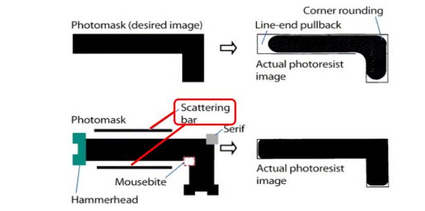
Optical Proximity Correction (OPC)
Scattering Bars (SB)
Double Patterning (DP) or Multiple Patterning
Phase Shift Masking (PSM)
Off-axis Illumination (OAI)
Optical Proximity Correction (OPC)
OPC is a Photo-lithography Enhancement technique commonly used to compensate the mask pattern for image errors due to diffraction or process effects (by reducing the value of the k1 factor in CD equation)
OPC is an effective way to deal with geometry distortion from design to chip; however, it does come at a price
First, there is the cost of the EDA tools you need to implement the OPC corrections
Second, you have an exponential increase in volume of the data representing the chip's layout, along with a huge increase in the time it takes to process this data and prepare it for photo-mask generation
Scattering Bars (SB)
Sub resolution assist features that improves the depth of focus of isolated features
Scattering Bars are added only for the most outer line of the dense pattern
Multiple Patterning
Involves decomposing the design across multiple masks to allow the printing of tighter pitches
38-nm features with 193-nm light water immersion lithography is the limitation with the current lithographic process
Multiple Patterning is a technique used in the lithographic process that can create the features less than 38nm at advanced process nodes
Multiple patterning basically changing the value of K1 in the Critical Dimension equation
Double Patterning
Double patterning counters the effects of diffraction in optical lithography
Diffraction effects makes it difficult to produce accurately defined deep sub-micron patterns using existing lighting sources and conventional masks
Diffraction effects makes sharp corners and edges become blur, and some small features on the mask won’t appear on the wafer at all
Double patterning is expensive because it uses two masks to define a layer that was defined with one at previous process nodes
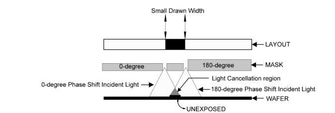
Phase Shift Masking (PSM) (not considered in PD)
Phase-shift masks are photo-masks that take advantage of the interference generated by phase differences to improve image resolution in photolithography
Controlling the phase enables constructive or destructive interference at desired locations in the image plane, thus sharpening or dulling the contrast as desired
These are photo-masks with structures that manipulate not only the amplitude of the transmitted waves but also their phase
Etching quartz from certain areas of the mask (alt-PSM) or replacing Chrome with phase shifting Molybdenum Silicide layer (attenuated embedded PSM) to improve CD control and increase resolution
There exist alternating and attenuated phase shift masks
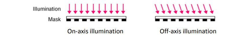
Off-Axis Illumination (OAI) (not considered in PD)
Off-axis illumination is one of the practical techniques to enhance resolution of a given optical system with bigger advantage of improvements in depth of focus
The specific illumination geometry is designed to enhance the contrast in the wafer plane of the photo-mask features whose dimensions are most Critical
With OAI, resolution of a given system can be improved without going for shorter wavelength or higher numerical aperture (NA)
This technique basically has no on-axis illumination component as oppose to partial coherence
The shape and size of the source plays an important role when different conditions of mask features such as density and orientation are considered
To obtain the highest resolution, illumination of the photo-mask is not performed by a discshaped source
The angular distribution of the illumination beam may have a complex structure, such as an annulus, a set of off-axis circles, or even a continuously varying profile