Explanation of Clock Skew Concepts
In simplest words, Clock Skew is the time difference between arrival of the same edge of a clock signal at the Clock pin of the capture flop and launch flop. Any signal takes some time to travel from one point to another. The time taken by Clock signal to reach from clock source to the clock pin of a particular flip flop is called as Clock latency. Clock skew can also be termed as the difference between the capture clock latency and the launch clock latency for a set of flops.

The above waveform was generated using Wavedrom. The code snippet to generate the above timing waverform is:
{ signal: [
{ name: "CLK", wave: "P.......",period: 2 },
{ name: "CLK", wave: "P.......",period:2, phase: -0.5 },
]}
The launch clock latency is 0ns and the capture clock latency is 2.5ns. The difference between the two is 2.5ns-0ns = 2.5ns which is the value of clock skew.
preCTS and postCTS skew values:
At pre-CTS stage, clock skew is a part of uncertainty. Ideally, the clock should reach clock pin of all the flip-flops present in a design at the same time i.e. the skew should be zero but this is not possible due to different wire-interconnect lengths and temperature variations.
Reason for Skew in a design: Just imagine a flip flop placed just close to the clock source and an another flip flop which placed at the far end of the core area. Due to the difference between the lengths of the interconnects, the skew cannot be zero in practical cases. To accommodate this, a user specified value is given to have accurate pre-CTS timing results.
After the clock tree is built, the actual skew values are available and the uncertainty only consists of Jitter value alone.

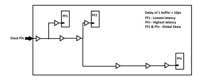
In the above diagram, Consider a flip-flop (FF1) which has the minimum latency and FFn which has the highest latency. Two terms can be defined from the above figure.
Local Skew: The latency difference between two related flops in a design is called as local skew. Suppose, FF1 (Launch flop) and FF2 (Capture flop) are two related flops.
Capture Clock Latency = 10+10+10+10 = 40ps
Launch Clock Latency = 10+10 = 20ps
Local Skew = 40-20= +20ps
Global Skew: The clock latency difference between two non related flops or the difference between the longest clock path and the shortest clock path in the design is called global skew. Suppose, FF1 has the minimum and FFn has the maximum value of clock latency in the design.
Maximum Clock Latency (FFn) = 60ps
Minimum Clock Latency (FF1) = 20ps
Global Skew = 60-20 = +40ps
Positive and Negative Skew:
Clock Skew = Capture Clock Latency (T2) - Launch Clock Latency (T1)
If T2>T1, Clock Skew is +ve
If T2,T1, Clock skew is -ve
If T2=T1, Clock skew is 0

In this scenario, the capture clock latency is more than the launch clock latency, and hence clock skew is positive. Positive skew is good for the setup timing. Since the capture clock is delayed by 2.5ns due to the addition of skew, the timing path has (1 clock period + Skew margin) to meet the setup requirement.
On the other hand, positive skew is bad for hold timing. Due to positive skew, the capture edge has shifted to the right. If the data path delay is less, in that case the data launched from the launch flop will reach the D pin of capture flop before the capture clock edge reaches the clock pin of capture flop which will result in the overwriting of the previous data stored at capture flop.

Negative Skew is good for hold timing because the new launch is delayed by skew value. Due to the delay of the new data launch, the previous data will be effectively captured and won't be overwritten. But at the same time, negative skew is bad for setup timing.
Useful Skew:
The skew which is purposely added in the design to meet the timing, especially in the clock paths where timing is failing so that timing is passed in that path. But useful skew cannot be added blindly. This needs to be done carefully by making sure the margin is available in previous and the next timing path. Uncontrolled addition of skew can lead to more timing violations instead of fixing them. It can be used to fix both setup and hold violations. Let's explain with the help of a simple example:

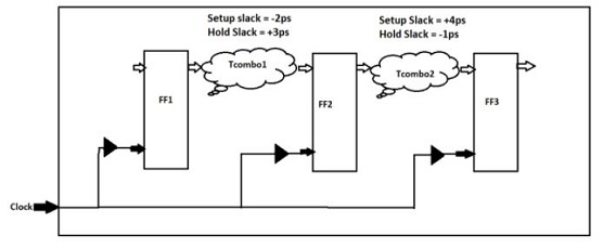
In the above circuit, for the simplification let's take the skew value to be zero. Due to the large value of Tcombo1, there is a setup violation of 2ps. Due to a small value of Tcombo2, the setup slack is +4ps but the hold is violating by 1ps. Now assume that the data path is fully optimized in both the stages. Since there is a positive hold slack of 3ps in the first stage and a positive setup slack of 4ps in the second stage, by using the slack margins both timing paths can be fixed. Here comes the concept of useful skew to meet timing.

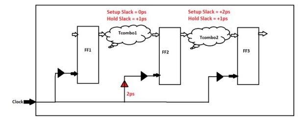
Let's add a buffer of delay 2ps in the Clock path of FF2 which will help in meeting the setup timing in the first path by pushing the capture clock. Since we have a good margin for setup slack in the second stage, it will not violate the setup time there.
The hold time was violating in the second path by 1ps which also got resolved because the buffer addition delayed the data launch in the second path by 2ps. Since we had a good margin for hold slack in the first stage, it will not violate the hold timing there. In this way, useful skew helps meeting timing.
Harmful Skew:
Where adding some skew to the failing paths can help in fixing timing violations, too much skew can cause violations.
If a large positive skew is added in the design, in that case, the capture clock will arrive after a long time and if the data path delay is small between the two flops, the data may reach the D pin of capture flop even before the capture edge reaches the clock pin of capture flop and may overwrite the previously latched data, resulting in Hold violation.
If a large negative is added in the design, in that case, the clock edge will reach the capture flop long before the launch flop. In this case, the new launch will be delayed. If the data path between the two flops is more, the launched data will get less to propagate to the D pin of capture flop and may reach very late resulting in Setup violation.
A hold violation is more dangerous than a setup violation as it cannot be fixed by decreasing the clock frequency.
What if there is actually zero skew in the design?

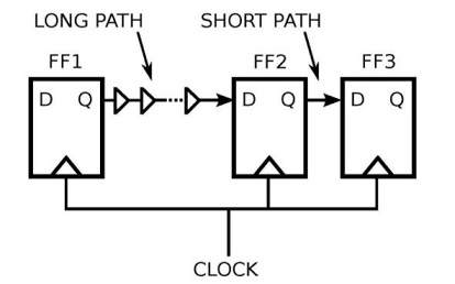
1. In the given figure, due to some Clock Jitter if the clock at FF3 gets delayed by a small interval of time, the new data launched by FF2 might reach D pin of FF3 very soon because of short path, resulting in the corruption of previous data at D pin of FF3, leading in Hold violation.
2. If the design has zero skew, which means all the flipflops in the design are getting clock at the same time. As we know, clock is the highest switching element in the design and a major contributor to the overall dynamic power consumption of the design. A chip consists of millions of flops. If all the flip flops switch at the same time, there will be a huge dynamic power dissipation in the design.
3. If one flip flop is placed closer to the clock source pin and another flip flop which is placed little far from the clock source pin, both are related, then to make the skew as zero, the tool would have added a large number of clock buffers and inverters in the clock path which will result in more area consumption and high utilization.
Disclaimer: This article is for educational purposes only. Opinions or points of view expressed in this article represent the views of the author. Feel free to comment if there is any correction required and any feedback is there.


